Color Computer Technical Reference Manual
The 6809E is one of the most powerful 8-bit microprocessors available. The architectural features include two 16-bit index registers, two 16-bit stack pointers, and two 8-bit accumulators. A block diagram of the 6809E CPU is shown in Figure 2.
FIGURE 2. 6809E BLOCK DIAGRAM
| -> | Buffers | --> | A0-15 | ||||||
| <-> | Buffers | <-> | D0-7 | ||||||
| v | |||||||||
| <-> | PC | <-> | Instruction register |
||||||
| <-- | U | <-> | |||||||
| <-> | S | <-> | v | ||||||
| <-- | Y | <-> | Interrupt Control |
<-- | !RESET | ||||
| <-- | X | <-> | <-- | !NMI | |||||
| <-- | D{ | A | <-> | <-- | !FIRQ | ||||
| B | <-> | <-- | !IRQ | ||||||
| <-- | DP | CC | <-> | ^ v | |||||
| v | Bus Control |
--> | LIC | ||||||
| ALU | <-> | --> | AVMA | ||||||
| --> | R/!W | ||||||||
| <-- | TSC | ||||||||
| <-- | HALT | ||||||||
| --> | BA | ||||||||
| ^ v | |||||||||
| Timing | <-- | E | |||||||
| <-- | Q | ||||||||
Figure 3 shows the programming model of the 6809E CPU. A and B are the two 8-bit accumulators. They are used for arithmetic operations and data manipulation. Also A and B may be combined to form the 16-bit register D, with A as the most significant byte. The Program Counter (PC) is used primarily for the CPU to keep track of its location in memory. X and Y are both 16-bit index registers. They are used by software to point to certain data or program segments in memory. The Hardware Stack Pointer (S) is used by the processor during subroutine calls and interrupts. Also available in the 6809E is the User Stack (U) which has all of the flexibility of the Hardware Stack, and is controlled exclusively by the programmer. In addition to all of the pointers and registers the 6809E also has a Direct Page Register (DP) and a Condition Code Register (CC). The Direct Page Register contents are used as the upper 8 bits of address when the direct addressing mode is used. This allows the direct mode to be used any place in memory. The Condition Code contains all of the arithmetic flags plus the mask bits for IRQ* and FIRQ*. These arithmetic flags are used to control all of the conditional branches. The mask bits allow the CPU to ignore all but the non-maskable Interrupt.
FIGURE 3. PROGRAMMING MODEL OF 6809E CPU
15 8 7 0 X Index register Y Index register U User Stack Pointer S Hardware Stack Pointer PC Program Counter D A B Accumulators DP Direct Page - - - - - - - - - 7 6 5 4 3 2 1 0 CCR E F H I N Z V C Condition Code Register | | | | | | | + Carry | | | | | | + - Overflow | | | | | + - - Zero | | | | + - - - Negative | | | + - - - - !IRQ Mask | | + - - - - - Half Carry | + - - - - - - !FIRQ + - - - - - - - Entire Flag
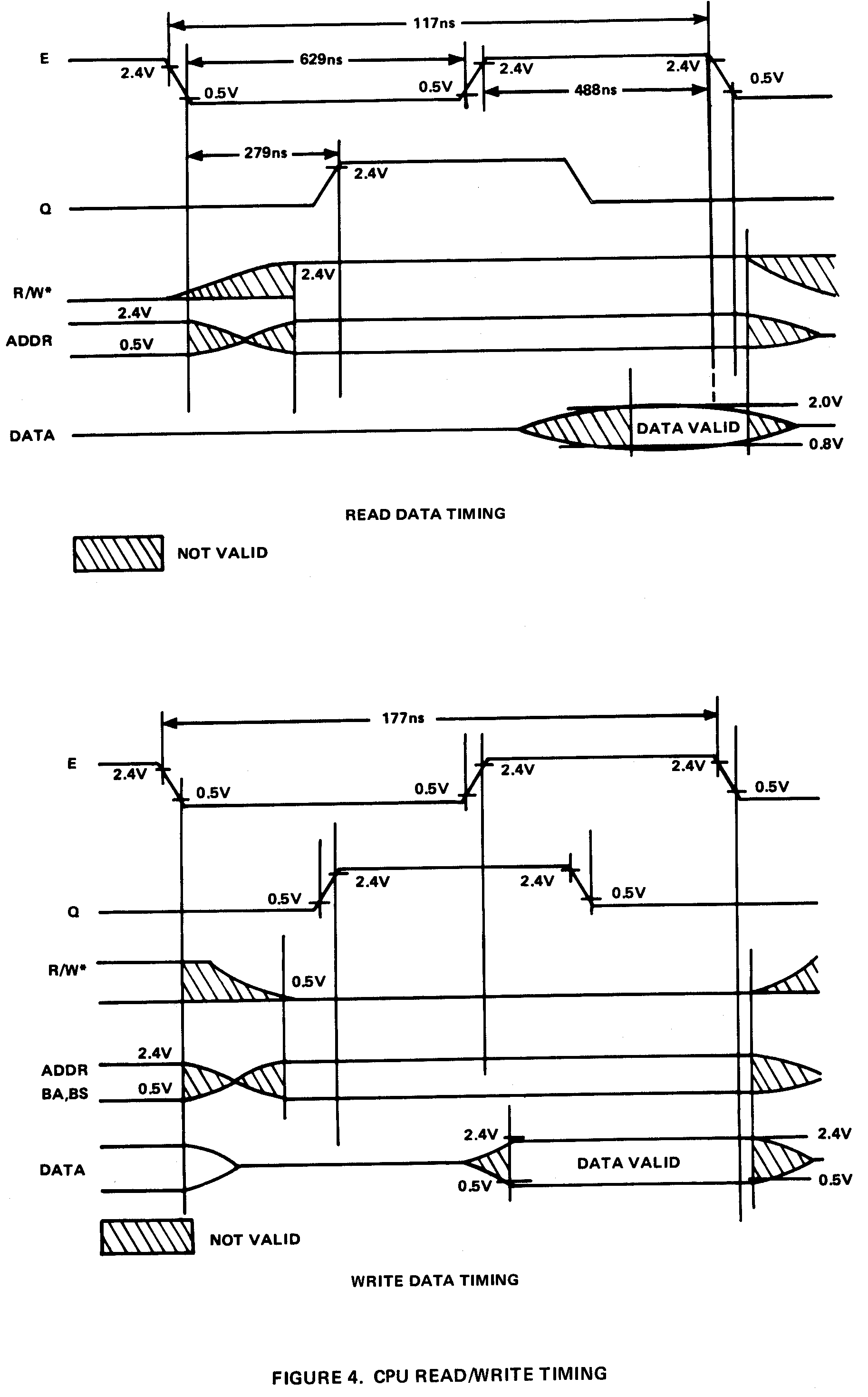
Figure 4 shows the typical timing for both the read and write cycle of the 6809E CPU. This timing is modified by Color Computer hardware during any access of the dynamic RAM. The address from the CPU will be provided to the RAM only while the E clock is high. This presents no problem as long as the RAM is sufficiently fast.
The 6809E CPU (U1) is a 40-pin IC. The Color Computer uses 34 of the 40 possible signals. Of the 34 signals, the life blood of the computer is the address and data lines. It is the duty of the address lines to select one address out of 65,536 possible locations. After the address has been selected, the data lines either input data to the CPU or output data to the selected location. The R/W* line (pin 32) is used to determine whether a read or write operation will occur. As long as the line is high the CPU is reading data. When it goes low the CPU is writing data.
In order for the 6809E CPU to function, two clock inputs must be provided, E and Q. These clocks are provided by U10, an MC6883 dynamic RAM Controller chip (SAM) and are 50% duty cycle clocks at a frequency of 0.89 MHz. As shown in Figure 4, Q is a quadrature clock signal which leads E by 90 degrees.
The other signals generated by U1 and used by the Color Computer are the Control/Interrupt pins. The RESET* (pin 37) indicates that a power-up or RESET has occured and the CPU will start over by executing the program addressed by the top two bytes of the BASIC ROM. This program is the Reset Routine that configures all of the programmable hardware in the Color Computer.
Three interrupt input pins are also used. IRQ* and FIRQ* are maskable interrupts which are connected to the PIA's and are used for multiple interrupt inputs. The non-maskable interrupt (NMI*) is reserved for Cartridge usage. All of these interrupt inputs use 4.7K pull-up resistors (R4, R5, and R6).
The last signal of the 6809E CPU used by the Color Computer is HALT (pin 40). This signal also requires a pull-up resistor (R3-4.7K). When the HALT* input is pulled low, the address bus, data bus, and R/W* line are all placed in the tri-state condition. This allows an external device to control the computer via the Cartridge connector.
Figure 4 CPU read / write timing
The reset circuitry is composed of R1, R2, C1, C40, CR1, CR2, and CR3. This circuit provides two different time duration pulses for power-up or reset. R1 and C40 provide a pulse of approximately 10 milliseconds which is used to reset the MC6883 memory controller chip (U10). The reset input to U10 is also used as an output, so diode CR2 is used to isolate the output signal on pin 7 from the reset circuitry.
The second reset pulse is the master system reset signal. This is provided to the CPU and both PIA's (U4 and U8). Cl and R2 provide this master reset pulse of approximately 0.1 sec. CR1 is used to isolate the two RC circuits. CR3 allows a quick discharge of C40 and C1 for rapid multiple resets.
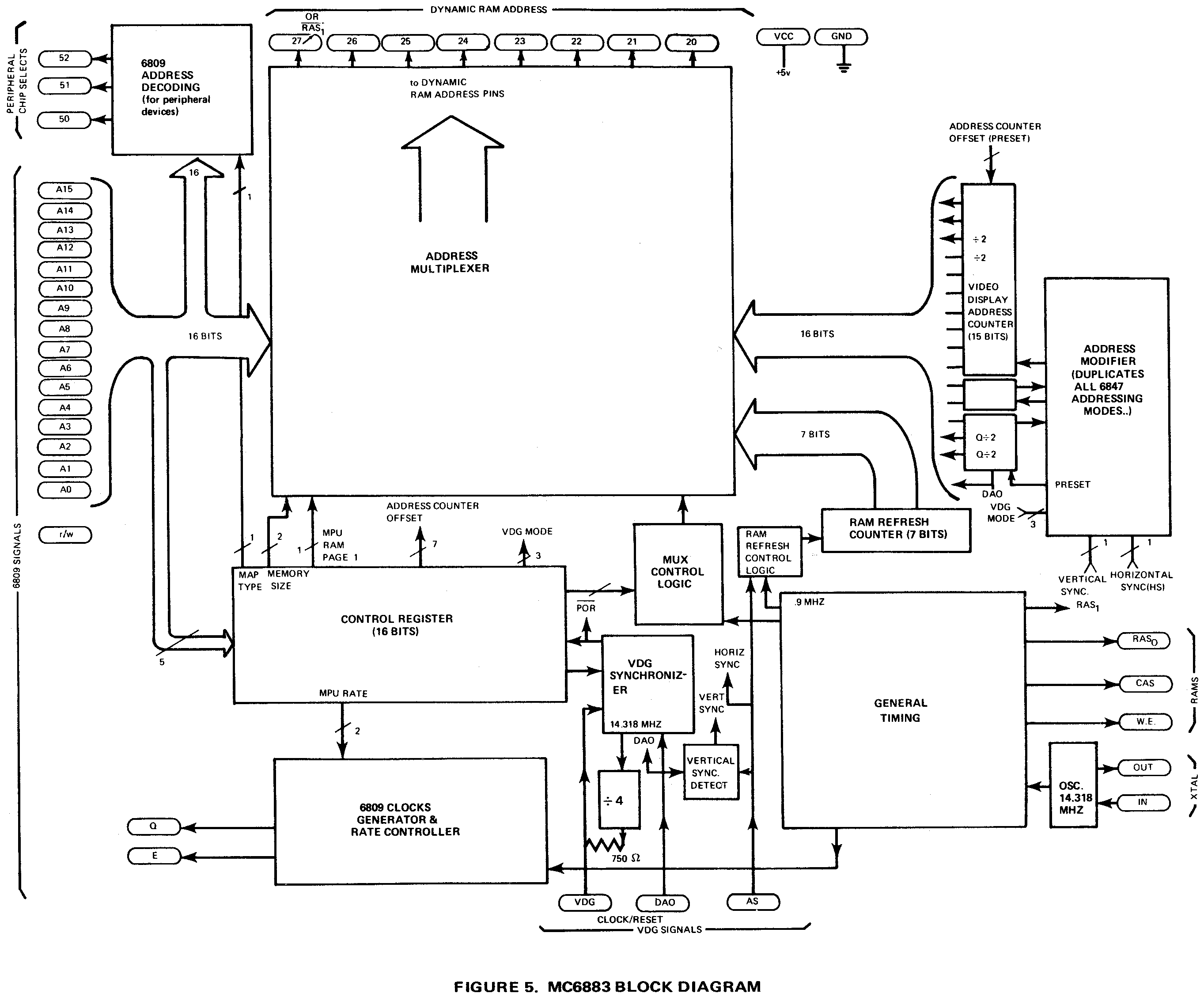
One of the most important chips in the Color Computer is the MC6883 (U10). This chip is a synchronous address multiplexer, sometimes referred to as SAM. SAM generates all of the system timing for the Color Computer and all of the device selection. In addition, it generates video address lines and multiplexes these with the CPU address lines for the dynamic memory. A functional block diagram of the MC6883 is shown in Figure 5.
To control this versatile chip, a 16-bit control register is used. These sixteen bits are divided as follows:
VDG ADDRESSING MODE	– 3 bits
VDG ADDRESS OFFSET	– 7 bits
PAGE SWITCH		– 1 bit
MPU RATE		– 2 bits
MEMORY SIZE		– 2 bits
MAP TYPE		– 1 bit
To set one of these bits, an odd address in the range of FFC0-FFDF is written to. To clear one of the bits, an even address in the same range is written to. The Memory Map (page 10) shows the breakdown of these bits.
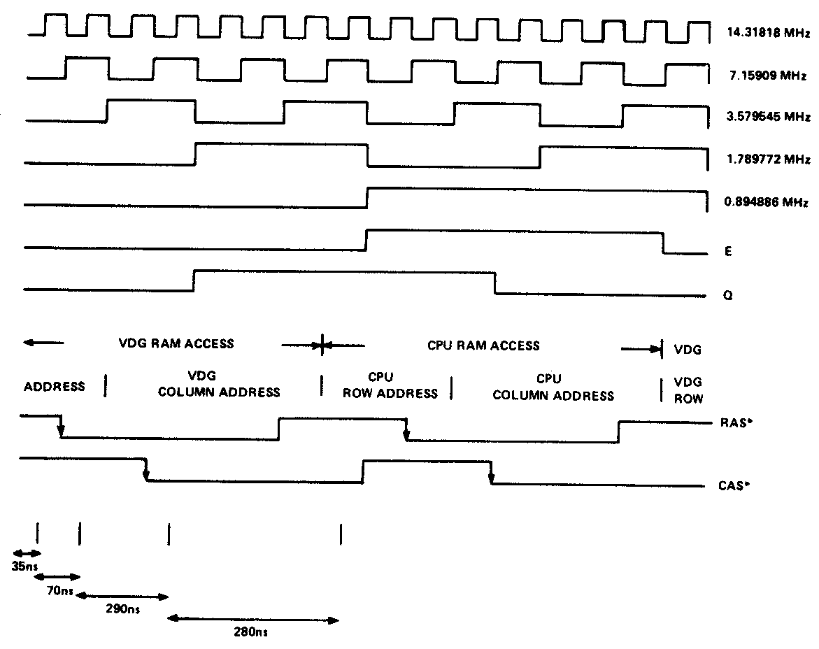
The Color Computer timing chain begins with the 14.31818 MHz oscillator composed of R43, Xl, C51, C4, and the internal oscillator in the MC6883. This is a series resonant circuit. C51 and C4 are used to exactly fix the frequency of the oscillation. C4 is a variable capacitor which allows minor frequency adjustments to compensate for device variation. C4 should be adjusted to give a video clock frequency of exactly 3.579545 MHz. R43 is used to control the voltage output of the oscillator.
From the master clock frequency of 14.31818 MHz, all of the System timing is derived. Figure 6 shows the breakdown of the master clock frequency to generate the timing signals. The video clock is exactly 14.31818 MHz/4 and must be the most accurate frequency in the Color Computer to provide a color picture. The next two signals, E and Q, are used by the CPU (U1). These signals are equal to the master clock divided by 16; a frequency of 0.89 MHz. The 0 signal leads the E signal by ninety degrees.
The E clock is the most important timing signal to the CPU and the multiplexing of RAM addresses roughly follows this signal. RAS* and CAS* are also triggered to occur at 0.89 MHz. RAS* strobes a row address into the dynamic RAM, and CAS* strobes a column address into RAM.
Figure 6 also shows the division of the RAM between the video address lines and the address lines from the CPU. During any CPU cycle, the RAM is only available to the CPU during the active portion of the E clock. However, this is sufficient if the RAM is capable of completing a Read or Write cycle during this time (the cycle time is a simple matter of specifying the correct access time for the RAM). The RAM is available to the video display during the low portion of the E clock (in actual fact, the display only requires the RAM during every other cycle of the E clock). To make this VIDEO/CPU multiplexing work, the MC6883 chip (U10) must keep the video display address lines in sync with the 6809E CPU (Ul) address lines; otherwise, a conflict could develop between the CPU and the video display. The sync process is accomplished immediately following reset by stopping the video clock until the VDG is in sync with the CPU.
The next major function of the MC6883 is address multiplexing for the dynamic RAM. First, the video address lines are reproduced, using FS*, HS*, DA0, and the VDG mode information (FS* is detected when DA0 is in the tri-state mode). These address lines are then added to the upper address lines from the address offset register to form the complete video address. The video address lines are then connected to the multiplexer bank. Also connected to the multiplexer bank is a 7-bit refresh counter. This 7-bit counter is used during horizontal sync to refresh the RAM. At other times this function is performed by the video address lines.
The multiplexer bank first selects either video/refresh address lines or CPU address lines. Next, the multiplexer selects between row and column address lines. The multiplexer then distinguishes between 4K, 16K, or 32K dynamic RAM's and presents the seven or eight address lines for the RAM's at the MC6883 output pins (pins 28 - 34).
The last major function of the MC6883 is device selection. The sixteen address lines from the CPU are used to select either the internal registers of the MC6883 or up to eight external devices. This memory map is shown in detail on pages 5 through 9. However, before the eight device selects leave the chip, they are multiplexed into three lines. At the output of the MC6883, a 74LS138 is used to de-multiplex the device selects. This 74LS138 (Ull) allows the Golor Computer to select between RAM, three sources of ROM, or the two PIA's. Also one NOR gate (U29 – 74LS02) is used to produce a clocked select signal for the ROM's and the RAM.
Figure 6: Color Computer Timing diagram
The Read Only Memories used in the Color Computer are simple digital devices requiring only data lines, address lines, and a chip select line. The chip select line turns on the ROM for operation. Then, one of 8,192 memory locations is accessed by the thirteen address lines. The eight data bits of stored information are then available at the data bus outputs for the CPU.
In the Color Computer, one or two 8K ROMs are used for the
BASIC Interpreter. To access these ROMs, the decoding circuitry
produces two chip select lines. The main BASIC ROM (U3) is
located at the Hexidecimal address A000-BFFF, The Expansion ROM
(U28) is located at the address 8000-
9FFF.
The primary portion of the video interface is shown on sheet 2 of the schematic diagram. The clock source for the video interface is the VDG CLK signal from the MC6883 chip (U10). This clock must be exactly 3.579545 MHz to generate a color signal for a TV. To operate properly, the VDG chip (U7) must be set to the correct mode by the control lines coming from PIA (U4). The VDG will then generate a display based on the data present on the input lines.
In the Color Computer, the memory address lines for the video display are supplied by the MC6883 chip (U10). To maintain synchronization with the VDG (U7), the horizontal sync signal and the LSB of the VDG address lines are connected to the MC6883 chip. In addition, the field sync signal is connected to the tri-state control of the VDG causing the address lines to enter a tri-state condition during vertical blanking. In total, thirteen video address lines are supplied to the RAM to support the maximum display size of 6K. The starting address of the display memory is located in the upper left corner of the display screen. As the television sweeps from left to right and top to bottom, the video address lines are incremented to produce the display.
The eight data input lines to the VDG are supplied by an octal latch. This latch is necessary to hold the output data for 16K RAM chips which have an unlatched output. In reality, this data is simply the contents of a portion of dynamic RAM.
The other VDG input lines used by the Color Computer are listed below.
MODE CONTROL A*/G – selects between alpha-semigraphics and full graphic modes.
MODE CONTROL A*/S – selects between alphanumerics and semigraphics. This line is connected to data bit 7.
MODE CONTROL INT*/EXT – used to select the semigraphic – 6 mode. This line is connected to the same PIA bit as GM0.
MODE CONTROL INV – selects between a black character on a green background or a green character on a black background. This line is connected to data bit 6.
MODE CONTROL GM0, GM1, & GM2 – these three lines are used to select one of eight full graphic modes.
CLOCK (CLK) – The VDG clock input (CLK) requires a 3.579545 MHz (standard) TV crystal frequency square wave.
THREE-STATE CONTROL – (MS*) is a TTL compatible input which, when low, forces the VDG address lines into a high impedance state.
The following output signals are used by the Color Computer.
LUMINANCE (Y) – this six level analog output contains composite sync, blanking, and four levels of video luminance.
ØA – This three level analog output is used in combination with ØB and Y outputs to specify one of eight colors.
ØB – This four level analog output is used in combination with ØA and Y outputs to specify one of eight colors. Additionally, one analog level is used to specify the time of the color burst reference signal.
CHROMA BIAS (CHB) – This pin is an analog output and provides a DC reference corresponding to the quiescent value of ØA and ØB. CHB is used to guarantee good thermal tracking and minimize the variation between the parts.
FIELD SYNC – (FS*) – The high to low transition of the FS* output coincides with the end of active display area. The low to high transition of FS* coincides with the trailing edge of the vertical synchronization pulse.
HORIZONTAL SYNC – (HS*) – The HS* pulse is synchronous with the horizontal synchronization pulse furnished to the television receiver by the VDG. The high to low transition of the HS* output coincides with the leading edge of the horizontal synchronization pulse.
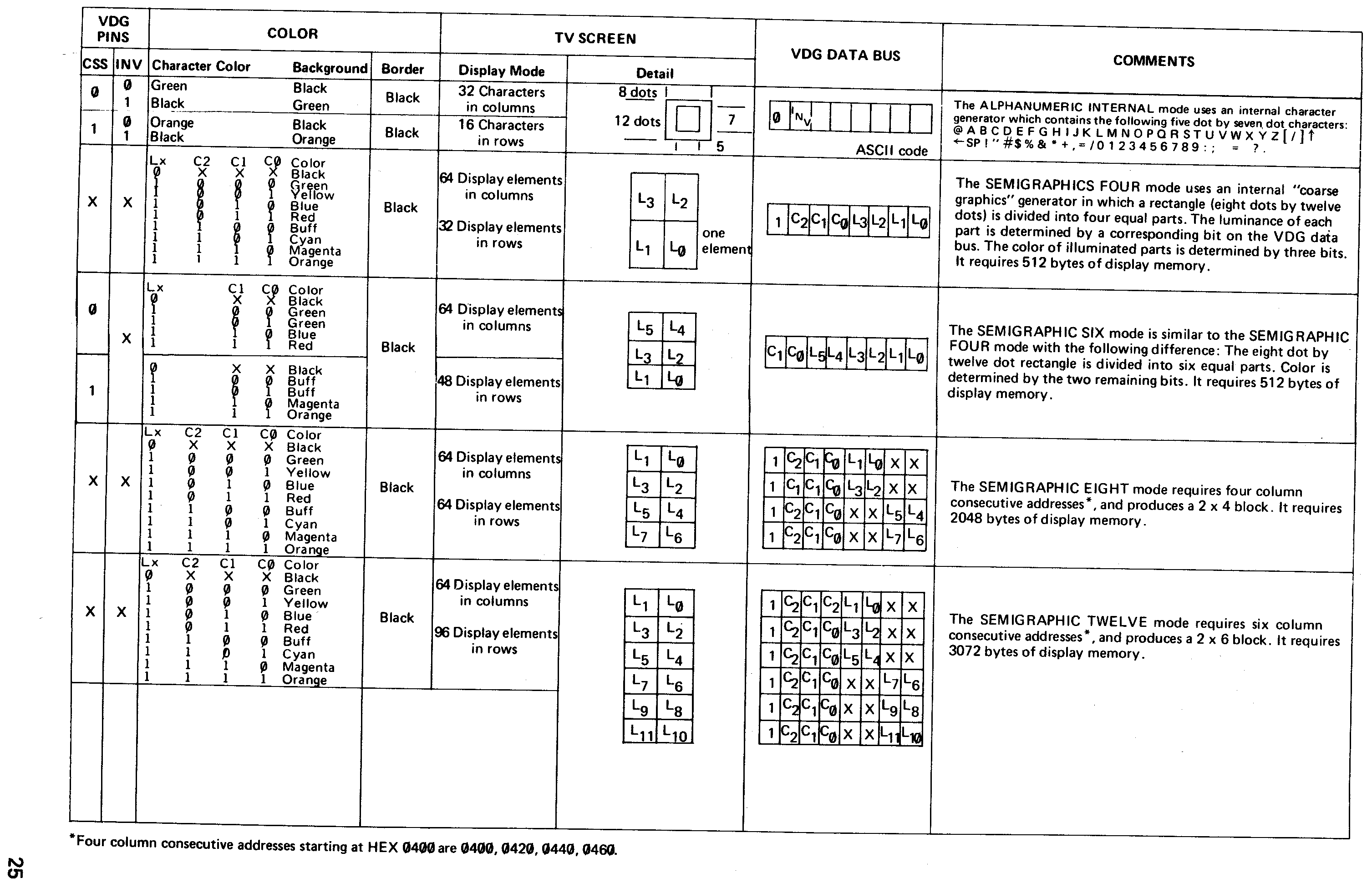
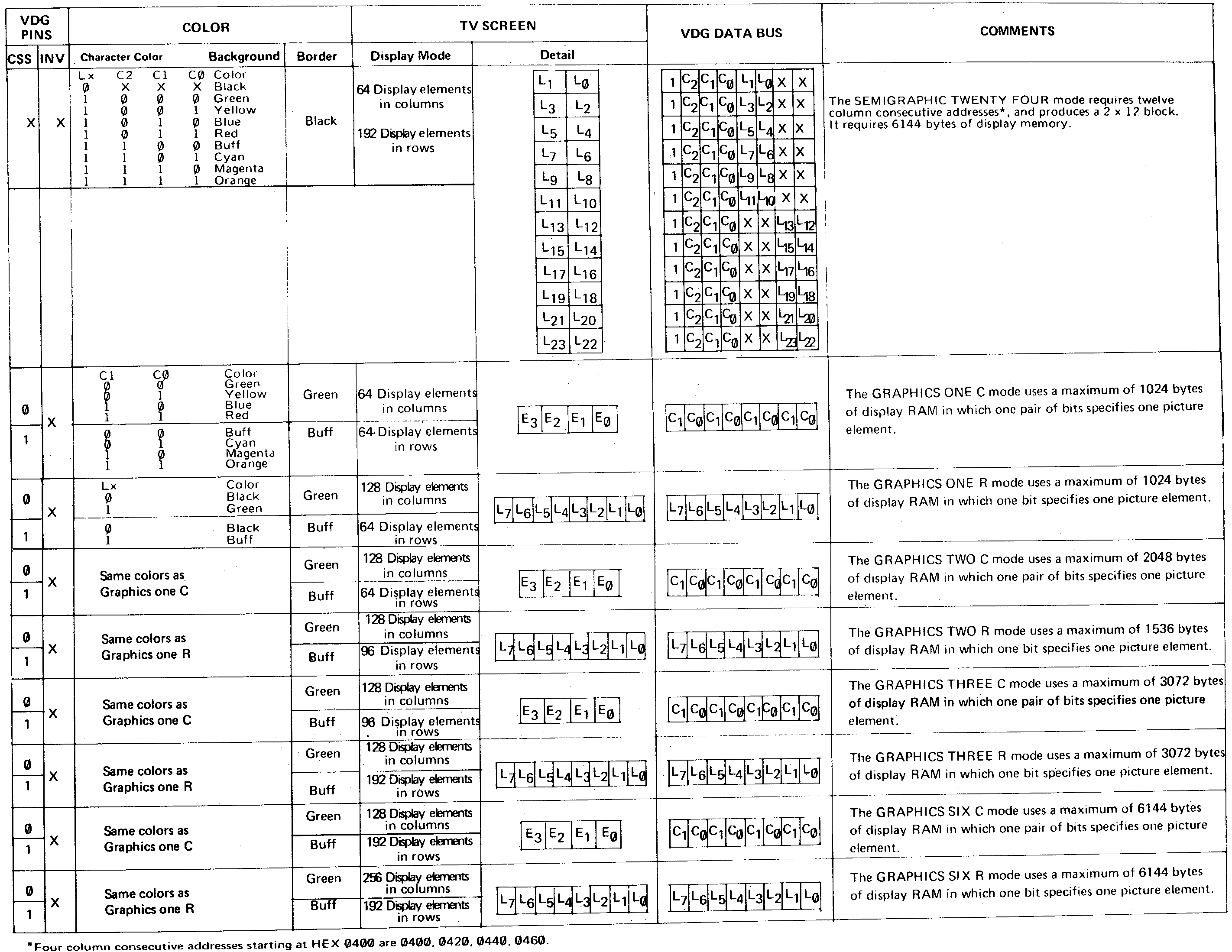
Together, the VDG (U7) and the MC6883 (U10) are capable of generating a large number of distinct display modes. Of this large quantity, fourteen separate Modes will be described. These include an alphanumeric, five semigraphic, and eight full graphic modes.
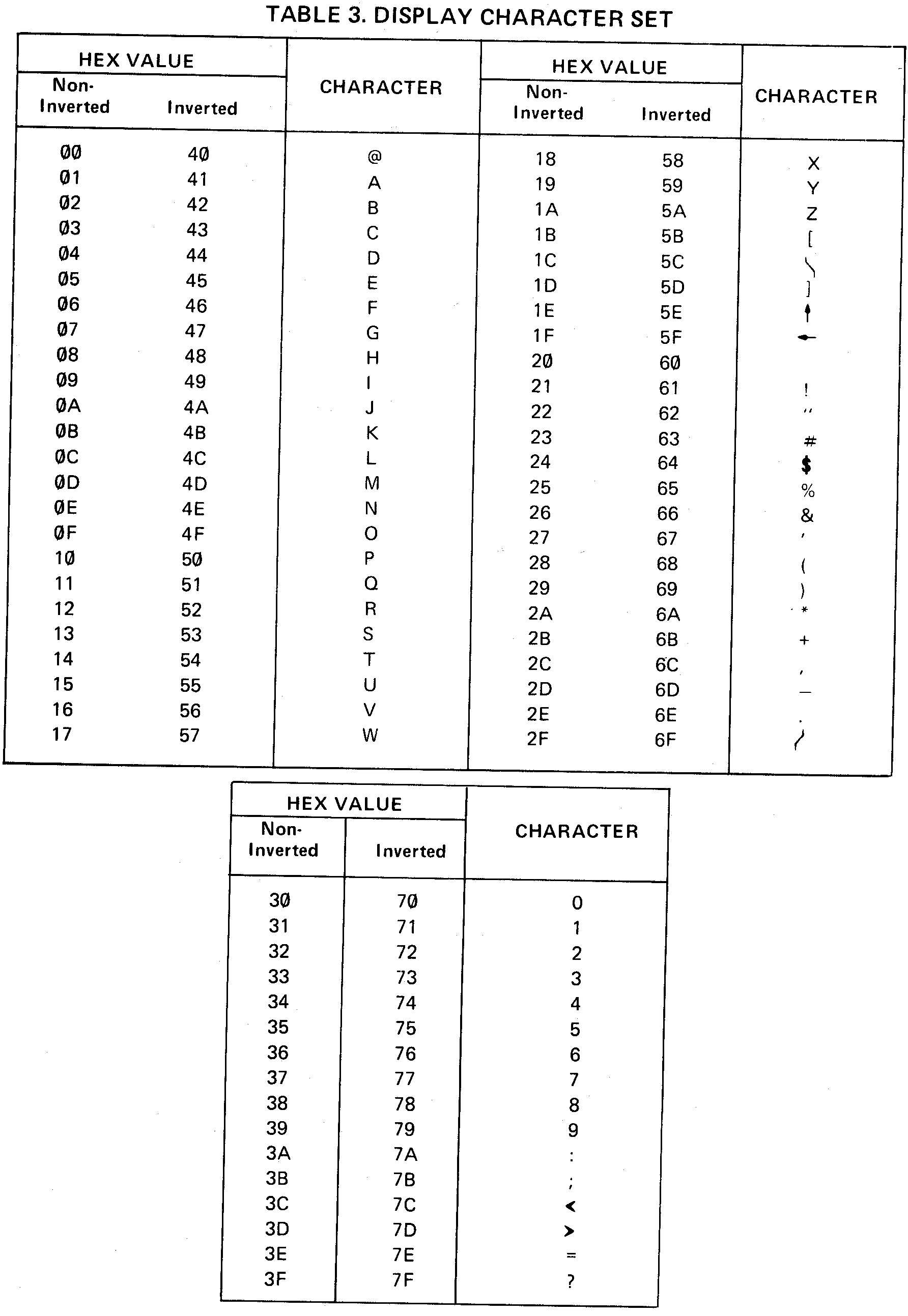
ALPHANUMERIC DISPLAY MODES – All alphanumeric modes occupy an 8 x 12 dot character matrix box and there are 32 x 16 character boxes per TV frame. Each horizontal dot (dot-clock) corresponds to one half the period duration of the 3.58 MHz clock and each vertical dot is one scan line. One of two colors for the lighted dots may be selected by the color set select pin (pin 39). An internal ROM will generate 64 ASCII display characters in a standard 5 x 7 box. Six bits of the eight-bit data word are used for the ASCII character generator and the two bits not used are used to implement inverse video and mode switching to semigraphics – 4, – 8, – 12, or – 24.
The ALPHA SEMIGRAPHICS – 4 mode translates bits 0 through 3 into a 4 x 6 dot element in the standard 8 x 12 dot box. Three data bits may be used to select one of eight colors for the entire character box. The extra bit is used to switch to alphanumeric. A 512 byte display memory is required. A density of 64 x 32 elements is available in the display area. The element area is four dot-clocks wide by six lines high.
The ALPHA SEMIGRAPHICS – 6 mode maps six 4 x 4 dot elements into the standard 8 x 12 dot alphanumeric box, a screen density of 64 x 48 elements is available. Six bits are used to generate this map and two data bits may be used to select one of four colors in the display box. A 512 byte display memory is required. The element area is four dot-clocks wide by four lines high.
The ALPHA SEMIGRAPHICS – 8 mode maps eight 4 x 3 dot elements into the standard 8 x 12 dot box. This mode requires four memory locations per box and each memory location may specify one of eight colors or black. A 2048 byte display memory is required. A density of 64 x 64 elements is available in the display area. The element area is four dot-clocks wide by three lines high.
The ALPHA SEMIGRAPHICS – 12 mode maps twelve 4 x 2 dot elements into the standard 8 x 12 dot box. This mode requires six memory locations per box and each memory location may specify one of eight colors or black. A 3072 byte display memory is required. A density of 64 x 96 elements is available in the display area. The element area is four dot-clocks wide by two lines high.
The ALPHA SEMIGRAPHICS – 24 mode maps twenty-four 4 x 1 dot elements into the standard 8 x 12 dot box. This mode requires twelve memory locations per box and each memory location may specify one of eight colors or black. A 6144 byte display memory is required. A density of 64 x 192 elements is available in the display are. The element area is four dot-clocks wide by one line high.
FULL GRAPHIC MODES – There are eight full graphic modes available from the VDG. These modes require 1K to 6K bytes of memory. The eight full-graphic modes include an outside color border in one of two colors depending upon the color set select pin (CSS). The CSS pin (pin 39) selects one of two sets of four colors in the four color graphic modes.
The 64 x 64 Color Graphics mode generates a display matrix of 64 elements wide by 64 elements high. Each element may be one of four colors. A 1K x 8 display memory is required. Each pixel equals four dot-clocks by three scan lines.
The 128 x 64 Graphics Mode generates a matrix 128 elements wide by 64 elements high. Each element may be either ON or OFF. However, the entire display may be one of two colors, selected by using the color set select pin. A 1K x 8 display memory is required. Each pixel equals two dot-clocks by three scan lines.
The 128 x 64 Color Graphics mode generates a display matrix 128 elements wide by 64 elements high. Each element may be one of four colors. A 2K x 8 display memory is required. Each pixel equals two dot-clocks by three scan lines.
The 128 x 96 Graphics mode generates a display matrix 128 elements wide by 96 elements high. Each element may be either ON or OFF. However, the entire display may be one of two colors selected by using the color select pin. A 2K x 8 display memory is required. Each pixel equals two dot-clocks by two scan lines.
The 128 x 96 Color Graphics mode generates a display 128 elements wide by 96 elements high. Each element may be one of four colors. A 3K x 8 display memory is required. Each pixel equals two dot-clocks by two scan lines.
The 128 x 192 Graphics mode generates a display matrix 128 elements wide by 192 elements high. Each element may be either ON or OFF, but the ON elements may be one of two colors selected with color set select pin. A 3K x 8 display memory is required. Each pixel equals two dot-clocks by one scan line.
The 128 x 192 Color Graphics mode generates a display 128 elements wide by 192 elements high. Each element may be one of four colors. A 6K x 8 display memory is required. A detailed description of the VDG modes is given in Table 2. Each pixel equals two dot-clocks by one scan line.
The 256 x 192 Graphics mode generates a display 256 elements wide by 192 elements high. Each element may be either ON or OFF, but the ON element may be one of two colors selected with the color set select pin. A 6K x 8 display memory is required. Each pixel equals one dot-clock by one scan line.
The following tables present mode programming information, a detailed description of the display modes, and the display character set.
TABLE 1. MODE SELECTION
| MC6883 DISPLAY MODE REGISTERS |
PIA
REGISTER BITS HEX ADDRESS FF22 |
DATA BITS |
ALPHA/GRAPHIC MODE SELECTED |
||||||||||
| V2 | V1 | V0 | 7 | 6 | 5 | 4 | 3 | 2 | 1 | 0 | 7 6 | ||
| 0 | 0 | 0 | 0 | X | X | 0 | CSS | N | N | N | 0 0 | Normal | Alphanumeric |
| 0 | CSS | 0 1 | Inverted | ||||||||||
| 0 | 0 | 0 | 0 | X | 1 X | Mode 4 | Semigraphics | ||||||
| 1 | CSS | Mode 6 | |||||||||||
| 0 | 1 | 0 | 0 | X | Mode 8 | ||||||||
| 1 | 0 | 0 | 0 | X | Mode 12 | ||||||||
| 1 | 1 | 0 | 0 | X | Mode 24 | ||||||||
| 0 | 0 | 1 | 1 | 0 | 0 | 0 | CSS | X X | 64 x 64 Color | Graphics | |||
| 0 | 0 | 1 | 0 | 0 | 1 | 128 x 64 Mono | |||||||
| 0 | 1 | 0 | 0 | 1 | 0 | 128 x 64 Color | |||||||
| 0 | 1 | 1 | 0 | 1 | 1 | 128 x 96 Mono | |||||||
| 1 | 0 | 0 | 1 | 0 | 0 | 128 x 96 Color | |||||||
| 1 | 0 | 1 | 1 | 0 | 1 | 128 x 192 Mono | |||||||
| 1 | 1 | 0 | 1 | 1 | 0 | 128 x 192 Color | |||||||
| 1 | 1 | 0 | 1 | 1 | 1 | 256 x 192 Mono | |||||||
X = DON'T CARE
N = DO NOT CHANGE
TABLE 2. DETAILED DESCRIPTION
OF DISPLAY MODES
TABLE 2. DETAILED
DESCRIPTION OF DISPLAY MODES (CONTINUED)
TABLE 3. DISPLAY CHARACTER SET
FIGURE 7. VDG VIDEO OUTPUT
At pin 28 of the VDG, the Y signal contains composite video and sync information. An example of this type of video signal is shown in Figure 7. This signal together with three color signals, CHB (pin 9), ØA (pin 11), and ØB (pin 10) is connected to the MC1372 color mixer chip (U12).
The MC1372 is a complete Color TV video modulator chip. However, for the Color Computer it is used only as a color mixer chip. Figure 8 shows a block diagram of the MC1372 chip. Pins 1 and 2 of the MC1372 form an oscillator circuit, but this is not needed in the Color Computer. The reference clock frequency of exactly 3.579545 MHz is produced by the MC6883 chip (U10). This signal is then rounded off by R17 and C53 before being connected to pin 2 of the MC1372 (U12). Pin 1 is left unconnected. Also, the duty cycle adjust input (pin 3) is left unconnected since a 50% duty cycle signal is produced by the MC6883.
The RF oscillator portion of the MC1372 is not required, so diode CR8 and resistor R20 are used to kill the oscillation. Also the orientation of CR8 controls the generation of normal or inverted video.
Using the color signals from the VDG, U12 produces the chroma output at pin 8. This signal consists of the reference color burst and the video color information. The MC1372 requires this signal to be AC coupled to pin 10. This is accomplished by capacitor C42. Resistor R18 determines the Luminance to Chrominance ratio.
The complete color video signal is available at pin 12 of the MC1372. However, at this point the signal has no drive capability and must be amplified before it can drive the modulator. This amplification is accomplished by Q1 and the associated circuitry. The video amplifier is powered by 8 volts DC. This power supply is produced off of the +12V supply by zener diode CR16, (a 3.9 volt zener diode). R69 is used to stabilize the zener voltage while C12 and C25 filter the voltage. This 8V supply is then connected to the collector of the transistor (Q1), and through a 3.9K pullup to the video output pin of the MC1372 (pin 12).
The video amplifier is a common collector amplifier designed to provide current gain. R19 and RS form a voltage divider for the video input signal. R9 and R21 are used to modify the voltage divider to compensate for variations in the output voltage of the MC1372. R46 is a bootstrap resistor used to provide as much current gain from the amplifier as possible. R47 is a biasing resistor for the amplifier.
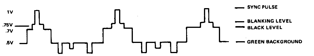
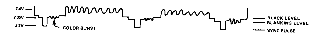
The video output from the emitter of Q1 is connected directly to pin 1 of the UM1285-8 modulator (U5). This signal should be adjusted with R21 so that the blanking level is exactly 2.35V. A sample of this video signal is shown in Figure 9.
FIGURE 8. MC1372 BLOCK DIAGRAM
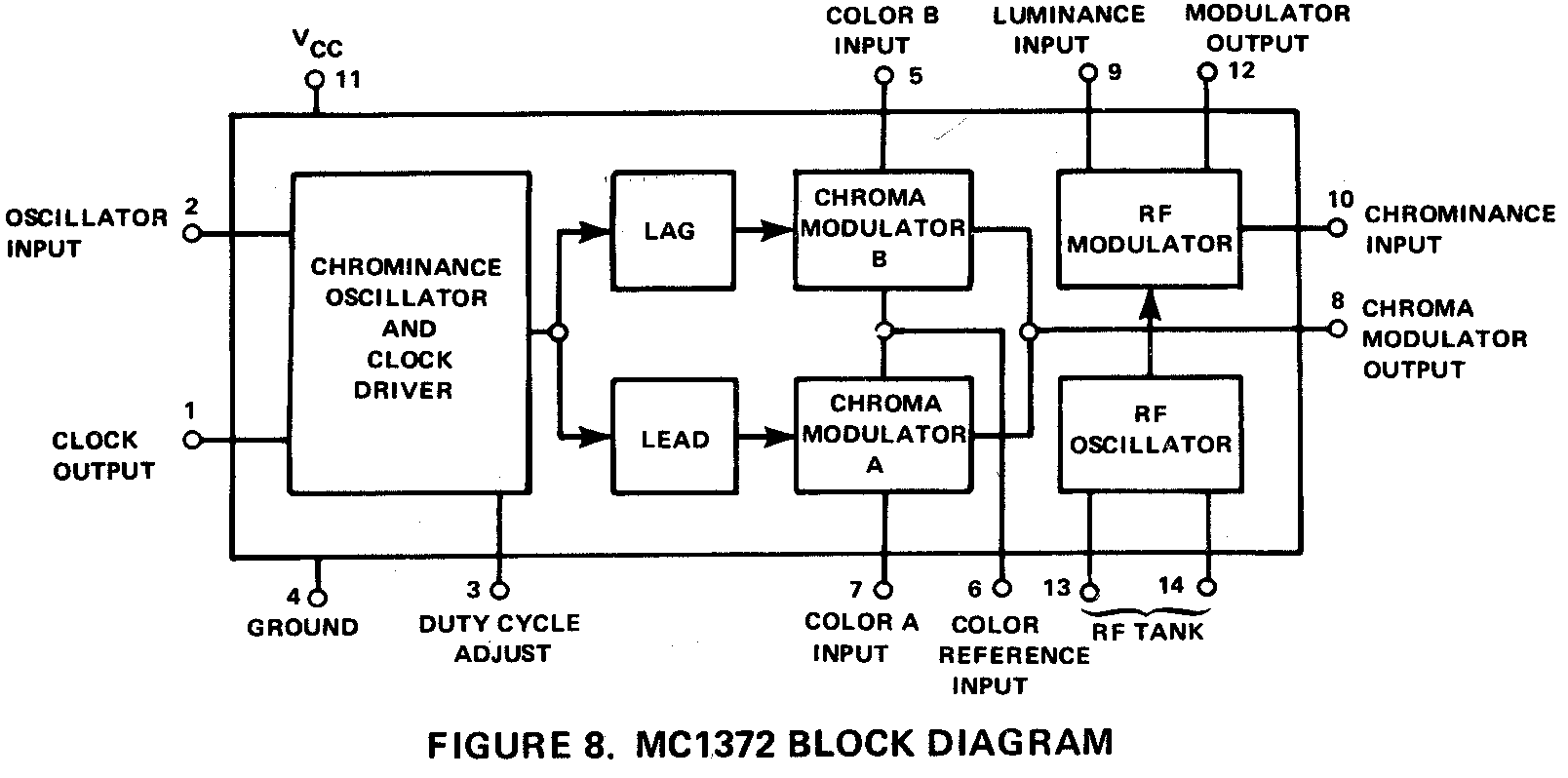
FIGURE 9. VIDEO INPUT TO THE MODULATOR
The UM1285-8 modulator is a high performance intercarrier vestigial sideband unit. The modulator is powered off the 12-volt supply with an inline current limiting resistor, R45. The modulator also has sound capability which is used by the Color Computer. The last input to the modulator is the channel select switch (S3). Channel 4 is selected by allowing the input to float high. Channel 3 is selected by ground.
Internal to the modulator, the DC sound input signal is converted to a 4.5 MHz frequency modulated signal. This signal is then mixed with the video and used to modulate the RF signal for the selected channel (61.25 MHz for Channel 3 or 67.25 MHz for channel 4). This final output is available at the phone jack connector of the modulator.
The Color Computer uses two peripheral interface adapters (PIA's). These devices provide a universal interface to the 6809E CPU chip, and they support all of the I/O functions in the Color Computer.
The functional configuration of the PIA is programmed by the CPU during the reset routine. Each of the peripheral data lines may be programmed to act as an input or output, and each of four control/interrupt lines may be programmed for one of several control modes. Figure 10 shows a block diagram of a PIA.
As shown in the block diagram, a PIA consists of two 8-bit data registers and 4 control/interrupt lines. The two 8-bit data registers are controlled by two data direction registers. These direction control registers are set up by the reset routine and normally will not be changed.
FIGURE 10. PIA BLOCK DIAGRAM
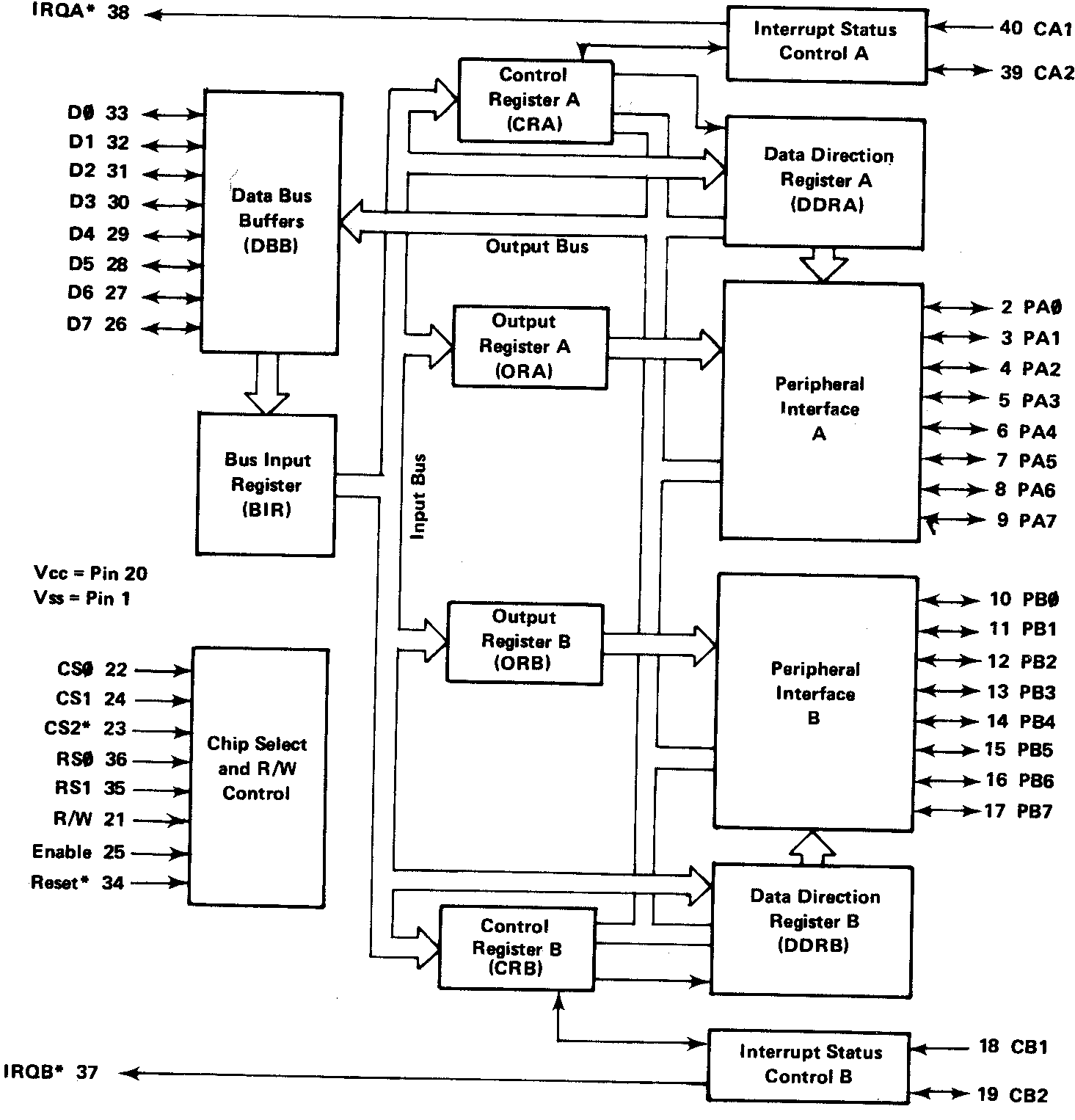
The four control/interrupt lines are controlled by the two control registers. The control registers also handle device selection within the PIA. Two of the four lines function only as interrupt inputs, and the other two lines may be used as interrupt inputs or outputs.
PIA U8 is used mainly for the keyboard. Data register B (pins 10-17) is programmed as an output, and is used to strobe the keyboard columns. The first seven lines of data register A (pins 2-8) are programmed as inputs and are used to read the keyboard rows. Pins 2 and 3 are also used as fire button inputs for the joysticks.
The other pins of PIA U8 serve various functions. Data register A (pin 9) is programmed as an input for the joystick interface. CA2 and CB2 (pins 19 and 39) are used as outputs. These two lines select one of four joystick or sound inputs. The last two pins of PIA U8, CA1 (pin 40) and CB1 (pin 18), are used as interrupt inputs. They are both tied to video clock outputs from the VDG (U7). If enabled, CA1 provides an interrupt after each video line. CB1, if enabled, provides an interrupt after each screen of data (60 Hz).
PIA U4 is used for several different functions. Pins 4-9 of data register A are used for the 6-bit digital to analog converter. Pin 3 of register A is the signal RS232OUT. This signal is used to drive the printer and other devices. Pin 2 of register A is the input for data from the cassette. Pins 13-17 of data register B are used to control the selection of the various alphanumeric and graphic modes of the VDG. Pin 12 of register B is an input for the memory size jumper. Pin 11 of register S is the single bit sound output. Pin 10 is the RS232IN signal input pin.
The control and interrupt pins of PIA U4 also serve various functions. CA1 (pin 40) is the input for the signal CD (a status interrupt input for the RS232C interface). CA2 is an output used to control the cassette motor. CB1 is the cartridge interrupt input. Whenever a cartridge is inserted in the computer, this input will interrupt BASIC and jump to the program in the cartridge. Finally, CB2 is used as an output to enable sound from the analog multiplexer (U9).
A commonly used input/output (I/O) device in the Color Computer is the 6-bit digital to analog converter (D/A). This device is addressed as the six MSB's of Hexidecimal address FF20. It allows the 6-bit digital word to be converted to an analog voltage level between 0.25 volts and 4.75 volts.
The converter is composed of a CMOS buffer (U2) and six discrete resistors. The converter operates by acting as a simple voltage divider. That is, the high outputs represent +5 volts and the low outputs, ground. The voltage is then determined by obtaining the parallel equivalent of the resistors tied high, the parallel equivalent of all the resistors (approximately 5K), and multiplying this ratio by 5 volts.
This simple picture is modified by three extra resistors (R72, R41, and R42). R72 is a 100K resistor connected to +5 volts, and the series equivalent of R41 and R42 forms a 100K resistor connected to ground. The effect of these resistors is to limit the minimum voltage to +0.25 volts and the maximum voltage to +4.75 volts. Also, C52 is included to filter the output voltage. For simplicity, the approximate output voltage may be calculated by the following formula:
VOLTAGE = (N x 0.0715) + 0.25 N = the 6-bit value (0-63}
One important usage of the D/A converter is with the joystick interface circuitry. This interface uses an analog multiplexer to select one of the four input joystick values. These values range between 0 and 5 volts, From the output of the multiplexer, the signal is directed to a comparator, which is also connected to the D/A converter. Then by a method of software successive approximation the joystick value may be determined to the 6-bit accuracy of the D/A converter.
Also provided in the joystick are two fire switches (momentary contact switches). One side of each switch is connected to ground, and the other side is connected to a PIA input. These two PIA inputs are also shared by rows 1 and 2 of the keyboard, so a conflict may exist if both are used at once, The PIA inputs are normally high so it is a simple software function to read the fire switches.
.Another important usage of the D/A converter is the sound output. This D/A converter is the primary source of sound effects for the computer, however three other sound sources are provided. These extra sound sources are a single bit sound source, sound from the cassette tape recorder, and sound from the cartridge.
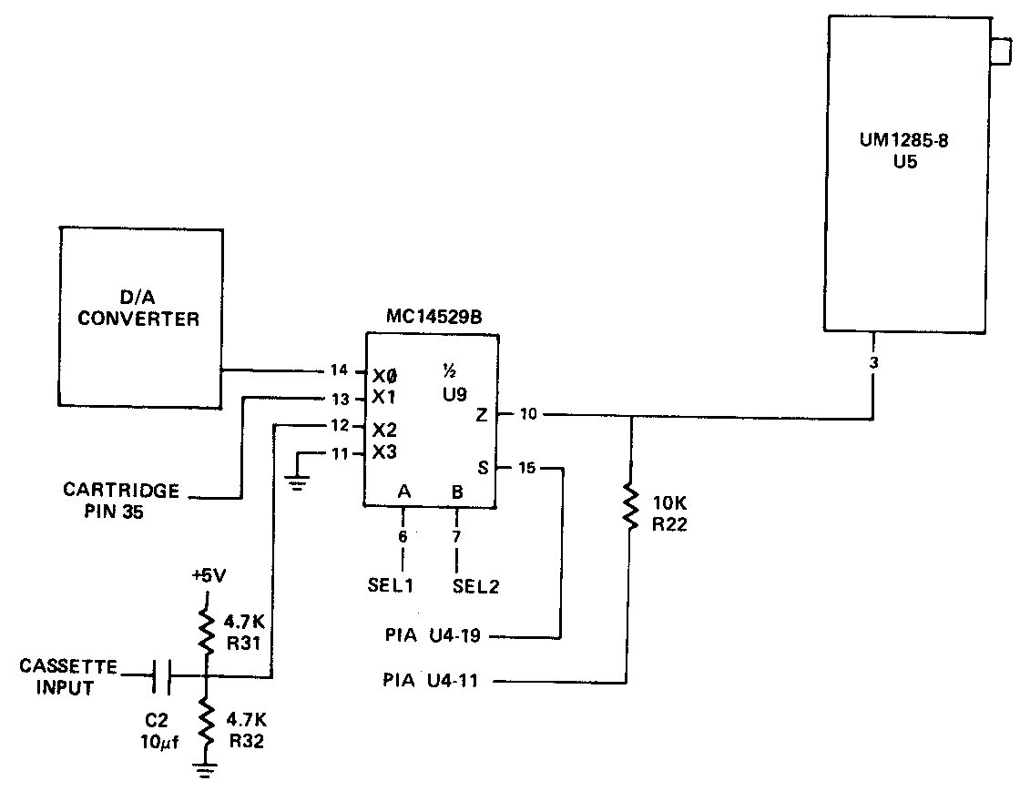
The D/A output is connected directly to the MC14529B analog multiplexer (U9). This chip is used to select one of three sound sources, and maybe disabled to allow use of the fourth single bit sound source. Table 4 shows the selection of the various sound sources. Figure 11 shows all of the circuitry for sound generation.
The cassette sound output must be modified before being connected to the analog multiplexer. For this purpose, a 10 uF non-polarized capacitor (C2) is used to level shift the signal. Also, two 4.7K resistors (R31 and R32) assign a DC level of 2.5 volts and limit the signal to 0 to 5 volts. This signal is then connected to the multiplexer (U9).
The output of the analog multiplexer is connected to pin 3 of the modulator (U5), and to the single bit sound source (pin 11, U4), which is isolated by a 10K resistor. At any time, only one of the two sources should be used, to avoid mixing the two sources.
TABLE 4. SOUND SELECTION
SNDEN
U9-15SEL 2
U9-7SEL 1
U9-6SOUND SOURCE SELECTED 1 0 0 6 BIT D/A 1 0 1 CASSETTE 1 1 0 CARTRIDGE 1 1 1 NOT USED 0 X X SINGLE BIT SOUND * NOTE: For single bit sound, PI A U4 pin 11 must be programmed as an output. It is normally programmed as an input.
X = DON'T CARE
0 = LOGIC LOW
1 = LOGIC HIGH
FIGURE 11. SOUND CIRCUITRY
The cassette interface is composed of an output attenuator connected to the 6-bit D/A, a motor control circuit, and an input zero crossing detector. However, most of the important cassette parameters are controlled by software.
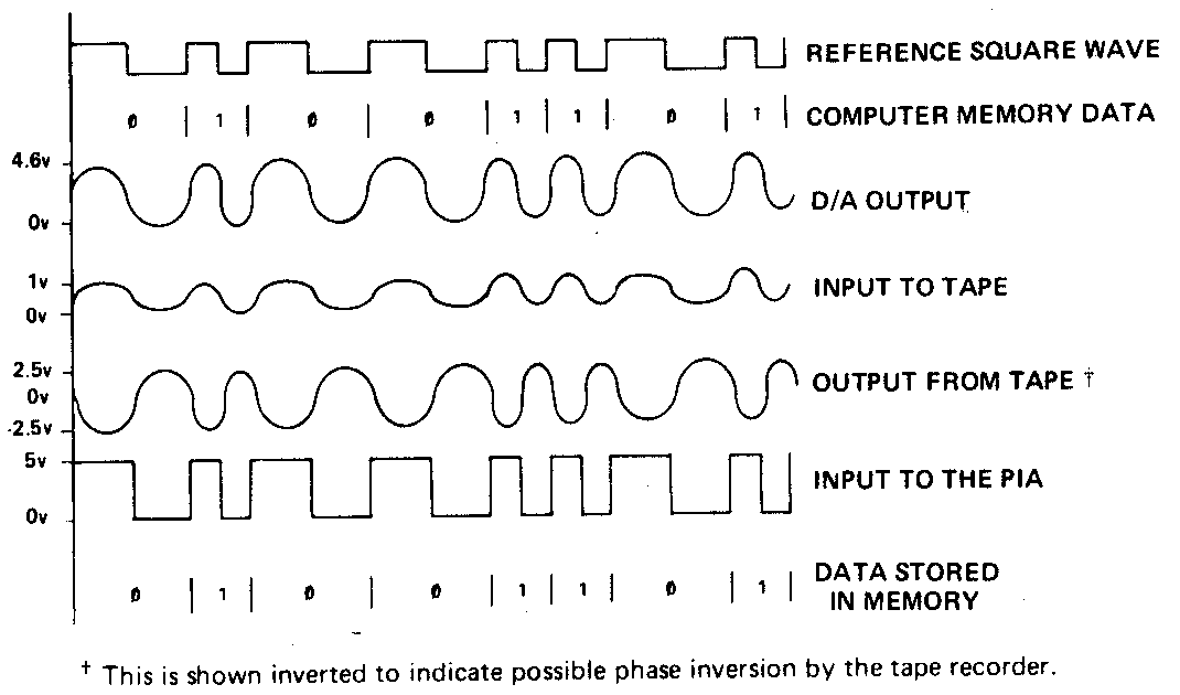
The cassette format chosen uses a sinewave of 2400 or 1200 Hertz to yield a Baud rate of approximately 1500 Baud. In this format, a 0 (or logic low) is represented by one cycle of 1200 Hertz, and a 1 (or logic high) is represented by one cycle of 2400 Hertz. A sample of data is shown in Figure 12. A typical program tape would consist of a leader of alternating 1's and 0's, followed by one or more blocks of data. A block of data is composed of 0 to 255 bytes of data with a checksum, sync byte, and the block length.
The output circuit utilizes the 6-bit D/A to generate a sinewave of 1200 or 2400 Baud. This signal is then attenuated to approximately 1 volt and connected to the auxiliary input of the cassette recorder.
This is shown inverted to indicate possible phase inversion by the tape recorder.
FIGURE 12. SAMPLE DATA OF CASSETTE FORMAT
The motor control circuit is controlled by an output PIA pin. This signal is used to switch transistor Q4. Q4 provides sufficient current capability to drive the relay coil. Diode CR7 is used to shunt voltage surges whenever Q4 is switched. Diodes CR9 and CR10 perform a similar function for the relay switch contacts. Whenever the relay contacts are opened or closed, a high voltage spike could occur. However, diodes CR9 and CR10 will shunt away any high voltage. C80 is provided to prevent RF noise associated with contact switching.
The input circuit is a zero crossing detector. R33 is a termination resistor for the cassette output. Resistors R37 and R38 are used to bias one input of the comparator at 1 volt. The other input is also biased at 1 volt by R36 and the series combination of R35 and R34. If the AC input from the recorder goes negative, diode CR4 turns on and sets the input to the comparator equal to 1/2 volt. Since the other input is biased at 1 volt, the comparator output is switched to the high state. If the AC input from the recorder is positive, diode CR4 is turned off and the input to the comparator will be at some point greater than 1 volt, in which case, the comparator output will be low.
The comparator output is open-collector, so pull-up resistor R40 is provided to generate a TTL signal. R39 is used to prevent oscillation of the comparator. The final portion of the cassette circuit is capacitor C81, which is used to isolate RF noise from the cassette cable.
The standard TRS80 Color Computer tape is composed of the following items:
The block format for Data blocks, Namefile blocks, or an End
of File block is as follows:
The End of File block is a standard block with a length of 0 and the block type equal to FFH.
The Namefile block is a standard block with a length of 15 bytes (0FH) and the block type equals 00H. The 15 bytes of data provide information to BASIC and are employed as described below:
The RS232C Interface utilizes a 4-pin DIN connector (P2). This interface allows the computer to have serial communication with printers, modems, or other computers. The four signals used by the interface are:
The pinout for the DIN connector is shown in Figure 13.
FIGURE 13. RS-232C CONNECTOR PIN-OUT
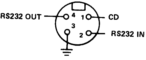
In general, an RS232C signal is defined as a high (or logic 1) if the voltage is greater than +3 volts. It is defined as a low (or logic 0) if the voltage is less than -3 volts. The range of -3 volts to +3 volts is undefined.
The RS232C interface circuitry is shown on sheet 2 of the Schematic, upper right corner. For the signal RS232OUT, an output pin of PIA U4 (pin 3) is tied to a 741C Op-amp (U15). The Op-amp is referenced at 1.4 volts by resistors R23 and R24. This reference causes the Op-amp to swing between the two power supply voltages (+/ – 12 volts) as the TTL input switches states. A 100 ohm resistor (R27) is included to provide a current limit on the output.
The two input signals (RS232IN and CD) utilize identical circuits. RS232IN (pin 2, U14) is tied to input pin 10 of PIA U4, and CD (pin l, U14) is tied to pin interrupt input 40 of PIA U4. The inputs from the external device are connected to the positive side of a diode. This diode blocks the application of a negative voltage to the comparator (U14). When a positive voltage is applied, the diode conducts, and the voltage is applied to the input. The comparator is referenced at 2 volts, thus if the input voltage is greater than 2.6 volts, the comparator is turned on.
The comparator output is open-collector so a pullup resistor is required for the output. Also a feedback resistor of 10M is used to prevent oscillation or ringing.
The components which make up the Keyboard Interface are shown on sheet 3 of the schematic, upper left corner. The PIA chip (U8) is the only digital circuit used. The PIA chip is a programmable interface device which functions as both an input and an output register. The eight keyboard columns are attached to the B side of the PIA. These eight lines are programmed to be outputs. The seven keyboard rows are attached to the A side of the PIA. These seven PIA lines are programmed to be inputs.
To read the keyboard, only one column is enabled by writing a zero in the bit that corresponds to that column and by writing ones in all the other bits. If a key has been pressed in that column, one of the input lines will be a zero and the key location will correspond to the bit that is low. By scanning each column in the keyboard, all of the keys may be checked.
The Color Computer requires four supply voltages: +12 volts, -12 volts, -5 volts, and +5 volts. The largest current requirement is on the +5 volt supply, therefore it is designed to provide up to 1.35 amp. The next largest requirement is 400 milliamps on the +12 volt supply. The requirements for -12 and -5 volts are very minimal, so the -5 volt supply is rated at 100 microamps and the -12 volt supply at 100 milliamps.
The power supply is shown on sheet 3 of the schematic diagram. On the primary side of the transformer, the power supply incorporates a 0.7 amp fuse and three high voltage capacitors. These capacitors (C20, C21, and C22) provide noise immunity and isolate computer noise. The two active lines of the power cord are connected across the primary side of the power transformer. The third line (ground) is connected to the computer ground.
The transformer has two center-tapped secondary windings. One secondary is rated at 16.3 volts AC at 1 amp, and is used solely for the 5 volt supply. The other secondary is rated at 33.5 volts AC at 0.35 amps. Both center taps are connected to ground. Each side of the 16.3 volt AC secondary is connected to a rectifier diode (CR12 and CR13). This produces a full-wave rectified signal when the two negative sides of the diodes are tied together.
All of the above circuitry is located on a secondary board inside of the Computer case. This isolates the high voltage AC signals away from the main circuit board. This transformer board is indicated on the schematic by a dashed line.
At the output of the transformer assembly, four signals are connected to the main board; ground, the input to the +5 volt regulator circuit, and the two sides of the 33.5 volt secondary. The two lines from the 33.5 volt secondary are connected to the bridge rectifier CR11.
At the output of bridge CR11, are three nearly identical regulator circuits. Each one uses a three terminal regulator chip to generate the DC supply voltages. C7 is the filter capacitor for the +12 volt supply. This is connected to U17 (a 78M12 regulator), and the + side of the bridge. CR14 provides protection for the regulator chip. C14 is the output capacitor for the +12 volt regulator. The negative side of the bridge is connected to filter capacitor C9. From C9, the -12 volt is identical to the +12 volt regulator circuit with the exception of C17. This capacitor is needed because two regulator circuits are sharing the same filter capacitor. The -5 volt regulator circuit is current limited by resistor R67. Also, due to the very low current, the protection diode and the large output capacitor have been eliminated.
Compared to the other regulator circuits, the +5 volt supply is a complex assortment of resistors, capacitors, and transistors. However, this circuit will provide a reliable 1.35 amp maximum current. The circuit begins with filter capacitor C10. Connected to C10 is the pass transistor Q2, and its bias resistor (R59). 02 controls the flow of current into the +5 volt line, but the actual job of regulation is performed by U13 (a 723C adjustable voltage regulator). The regulator output (pin 10) is buffered by Q3. Then Q3 is used to drive the base of pass transistor Q2.
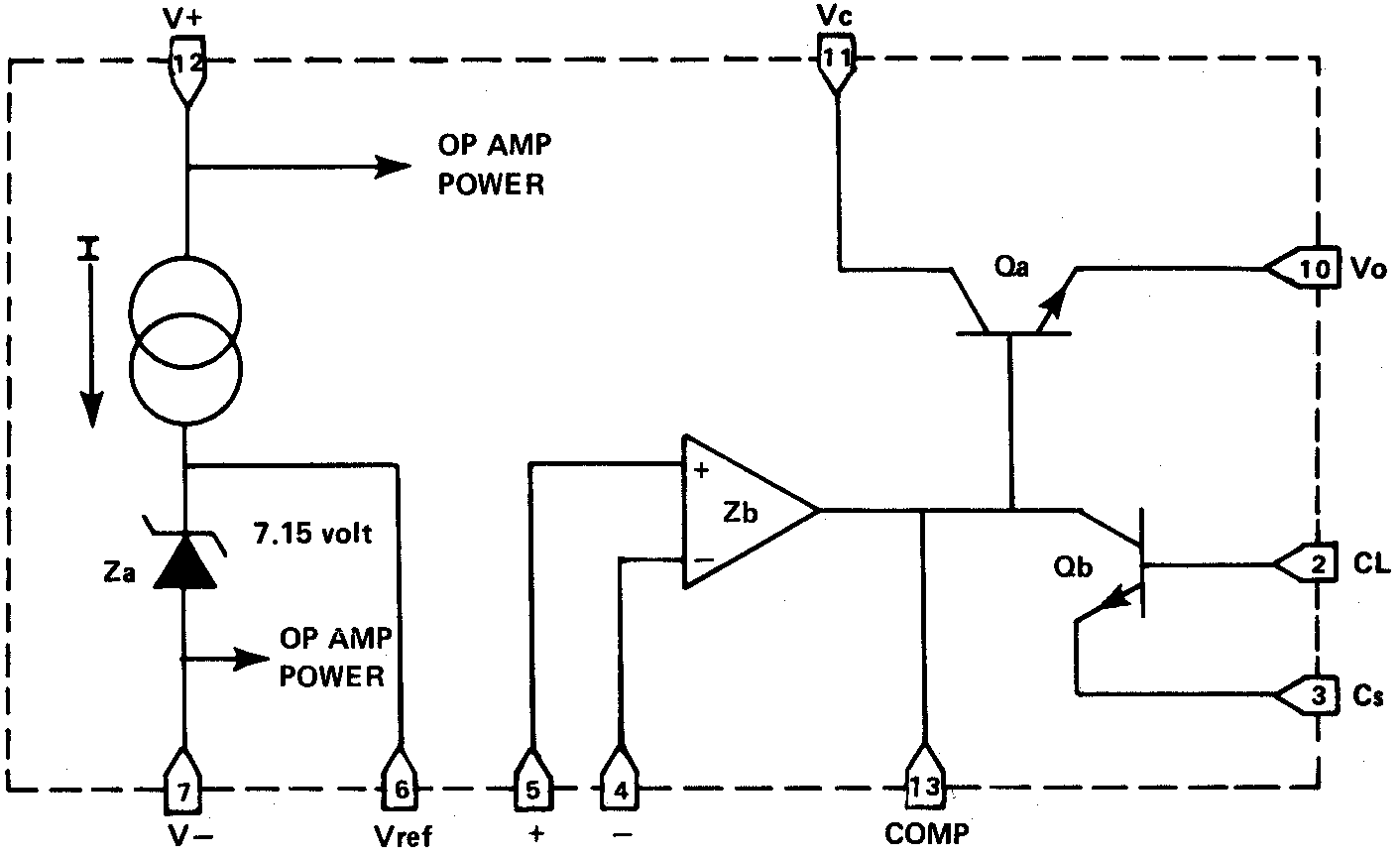
Figure 14 shows a Block diagram of the 723C regulator chip. The regulator is powered from the +12 volt supply. In operation, a 7.15 volt zener reference is available at pin 6. Resistors R60, R61, and R62 then divide this reference voltage down to 5 volts, which -is connected to pin 5 of the regulator. Pin 5 is the non-inverting input to internal Op-amp Zb (as shown in Figure 14). The inverting input is connected through a feed-back resistor (R63) to the +5 volt output. Op-amp Zb is then turned on or off in response to changes on the 5 volt line. Cl1 is the frequency compensation capacitor for Zb.
The output from Op-amp Zb controls transistor Qa, which drives the regulator output. Qa is also powered from the +12 volt supply through resistor R58. There is also a second control source on Qa, which is transistor Qb. This transistor allows a current limit to be set by resistors R65 and R64. If the current limit is exceeded, Qb will turn on and turn off Qa.
Returning briefly to pass transistor Q2, the next component is R66, which limits the output current. Overvoltage protection is provided by CR17, a 6.2V zener diode. C16 is the output filter capacitor for the+5 volt supply.
FIGURE 14: 723 REGULATOR DIAGRAM
The 40-pin cartridge connector provides the possibility of expanding the TRS-80 Color Computer in almost any manner. All of the important CPU bus signals are tied to this connector. A complete list and brief description of these Signals is provided in Table 5.
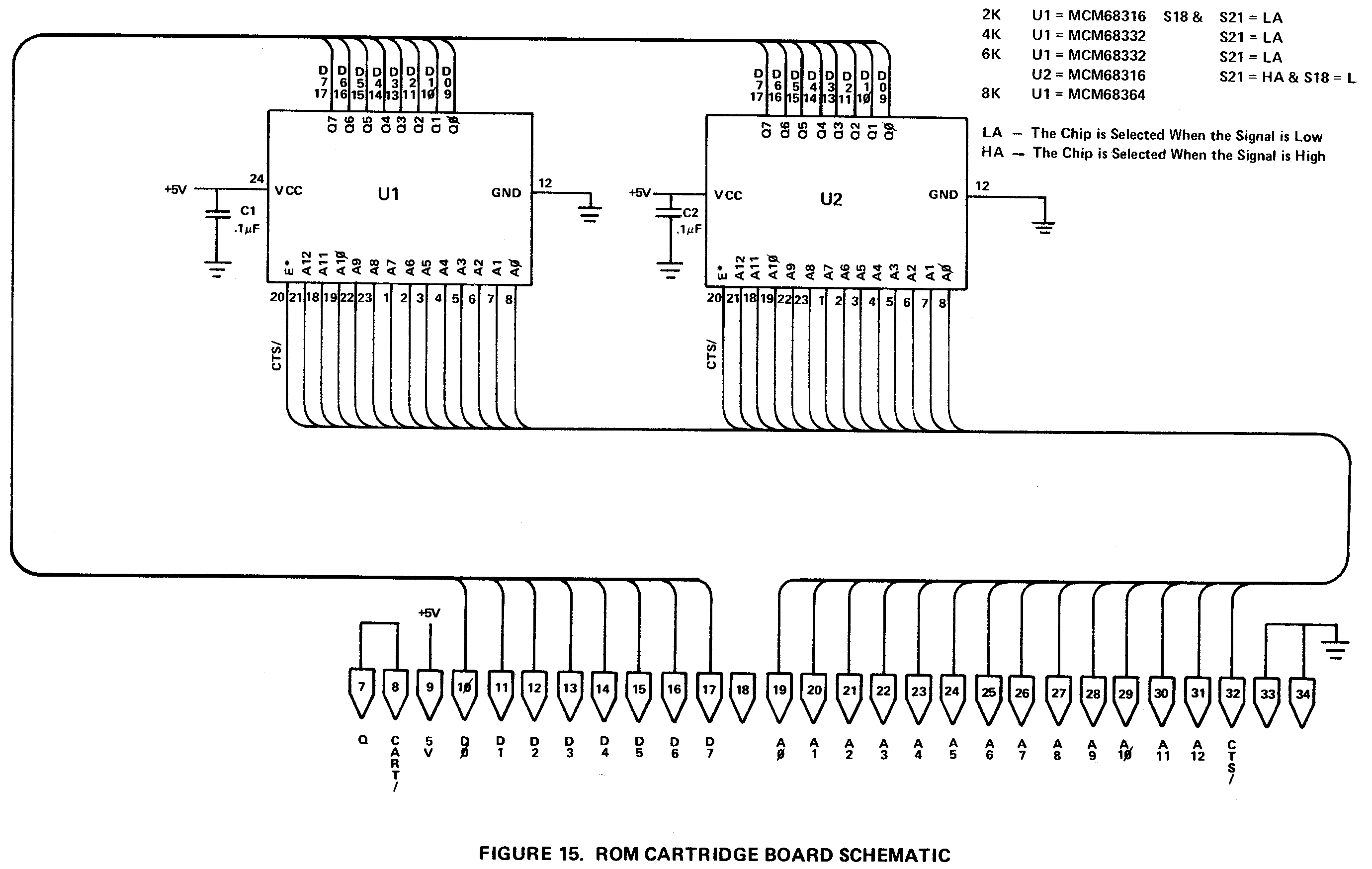
The most common usage of the cartridge connector is with the ROM Cartridge. A schematic of the ROM Cartridge board is Shown in Figure 15. In operation, U1 would be a 16K, 32K, or 64K ROM, and U2 might be a 16K or 32K ROM (the total of Ul and U2 must not be greater than 64K). For cartridge detection, the clock signal (0) is shorted to the cartridge interrupt pin. This generates an interrupt anytime the cartridge is plugged in and forces the computer to jump to the program in ROM.
In addition to the expected data, address, and R/W lines, several control and special purpose signals are available on the Cartridge connector. They are described in detail as follows:
| HALT* | This signal allows the data and address buses to be placed in the tri-state mode so an external processor may access RAM and ROM. |
| NMI* | This is the non-maskable interrupt input to the CPU. |
| RESET* | This is master system reset and power-up clear signal. |
| E & Q | These are the two clock signals for the 6809E CPU. |
| CART* | This is an interrupt input to one of the PIA'S. It is used to detect the presence of a Cartridge. |
| CTS* | This is the select signal to the Cartridge. The address space C000 (Hex) through FFEF (Hex) is selected. |
| SND | This signal is connected directly to the sound multiplexer, to allow a sound source in the cartridge. |
| SCS* | This is a spare divide select signal from U11. It selects the address space FF40 (Hex) through FF5F (Hex). |
| SLENB* | This signal disables the internal device selection. This allows decoded but unused sections of memory to be used by the Cartridge hardware. |
TABLE 5: CARTRIDGE CONNECTOR SIGNALS
PIN #	SIGNAL	DESCRIPTION
	NAME
1	-12 V	-12 Volts (100 MA)
2	+12 V	+12 Volts (300 MA)
3	HALT*	Halt Input to the CPU
4	NMI*	Non-Maskable Interrupt to the CPU*
5	RESET*	Main Reset And Power-Up Clear Signal To The System
6	E	Main CPU Clock (0.89 MHz)
7	Q	Quadrature Clock Signal Which Leads E
8	CART*	Interrupt Input For Cartridge Detection
9	+5V	+5 Volts (300 MA)
10	D0	CPU Data Bit 0
11	D1	CPU Data Bit 1
12	D2	CPU Data Bit 2
13	D3	CPU Data Bit 3
14	D4	CPU Data Bit 4
15	D5	CPU Data Bit 5
16	D6	CPU Data Bit 6
17	D7	CPU Data Bit 7
18	R/W*	CPU Read/Write Signal
19	A0	CPU Address Bit 0
20	A1	CPU Address Bit 1
21	A2	CPU Address Bit 2
22	A3	CPU Address Bit 3
23	A4	CPU Address Bit 4
24	A5	CPU Address Bit 5
25	A6	CPU Address Bit 6
26	A7	CPU Address Bit 7
27	A8	CPU Address Bit 8
28	A9	CPU Address Bit 9
29	A10	CPU Address Bit 10
30	A11	CPU Address Bit 11
31	A12	CPU Address Bit 12
32	CTS*	Cartridge Select Signal
33	GND	Signal Ground
34	GND	Signal Ground
35	SND	Sound Input
36	SCS*	Spare Select Signal
37	A13	CPU Address Bit 13
38	A14	CPU Address Bit 14
39	A15	CPU Address Bit 15
40	SLENB*	Input To Disable Device Selection
Figure 15: ROM CARTRIDGE BOARD SCHEMATIC
The RS232C Interface hardware in the Color Computer is capable of communication with any device which will operate with the minimum three signal interface. It is also possible that devices which use a larger set of RS232C signals may be used with the Color Computer. This would be accomplished by connecting unused device inputs to the correct high or low level.
In software, the only RS-232C device supported by the 8K BASIC ROM is a serial printer. For use with the printer, the pin assignment of P2 differs from that listed in the RS232C Interface section.
Pin 1 is not used.
Pin 2 is connected to the busy output (or status line) of the printer.
Pin 3 is ground.
Pin 4 is the computer output to the printer.
If your printer does not provide a status line, then pin 2 must be connected to a positive voltage of +3 volts or greater (up to the maximum +12 volts). This tells the computer that the printer is ready all of the time.
In order to operate, the software must make several assumptions about the printer. These assumptions are:
Some printers will require that these assumptions be modified.
This may be accomplished by changing RAM variables or by a
special driver routine.
A list of all of the printer variables is given in Table 6. Also, Table 7 lists some alternate values for these variables. The last comma field variable (2) should be set equal to the width value minus the comma field width. The comma field width will normally stay at 16.
NOTES:
(1) In Revision 1.1 ROMs this format has been
changed from seven to eight data bits.
(2) Comma field is the number of spaces allowed to
print a variable value.
TABLE 6: LINE PRINTER VARIABLES
						INITIAL VALUE
			HEXADECIMAL	DECIMAL HEXA
VARIABLE		ADDRESS		ADDRESS DECIMAL DECIMAL

BAUD RATE MSB		0095		149	00	  0
BAUD RATE LSB		0096		150	57	 87
LINE DELAY MSB		0097		151	00	  0
LINE DELAY LSB		0098		152	01	  1
COMMA FIELD WIDTH	0099		153	10	 16
LAST COMMA FIELD	009A		154	70	112
LINE PRINTER WIDTH	009B		155	84	132
TABLE 7: ALTERNATE LINE PRINTER VARIABLE VALUES
BAUD RATE:	DECIMAL VALUE	HEXADECIMAL VALUE
		MSB    LSB	MSB     LSB
120 BAUD	1	202	01	CA
300 BAUD	0	180	00	BE
600 BAUD	0	 87	00	57
1200 BAUD	0	 41	00	29
2400 BAUD	0	 18	00	12
LINE DELAY:	DECIMAL VALUE	HEXADECIMAL VALUE
		MSB    LSB	MSB     LSB
 .288 SECONDS	 64	  00	40	00
 .576 SECONDS	128	  00	80	00
1.15 SECONDS	255	255	FF	FF
WIDTH:			DECIMAL VALUE	HEXADECIMAL VALUE
16 CHARACTERS/LINE	 16		10
32 CHARACTERS/LINE	 32		20
64 CHARACTERS/LINE	 64		40
255 CHARACTERS/LINE	255		FF
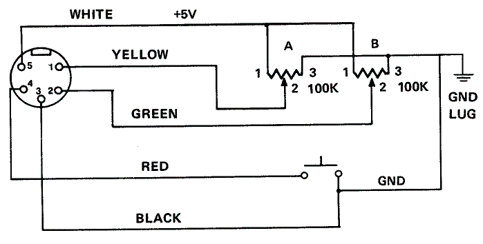
The joysticks are two identical assemblies which will plug into either P3 or P4. Figure 16 shows a schematic of the joystick assembly. It consists simply of a push button switch for the fire switch and the dual potentiometers connected by a mechanical assembly.
The mechanical assembly causes both potentiometers to be changed at the same time. This gives the effect of a two-dimensional control. The potentiometers are connected so that 5 volts is applied to one side of the variable resistor, and ground is connected to the other. This allows the center wiper to vary from 0 to 5 volts as the handle is moved. The push button switch merely provides a momentary ground contact for an input signal.
FIGURE 16: JOYSTICK SCHEMATIC
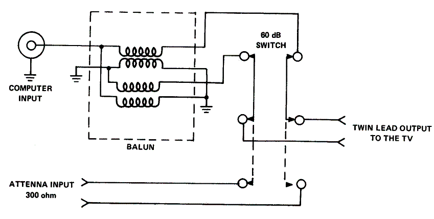
The antenna switch box consists of a switch and a balun, with connectors provided for attachment to the computer, the TV antenna, and the home TV. The switch box is connected to the customer's TV, through the 300 ohm twin lead output. The TV antenna is attached directly to the switch box. The computer output is connected through a 75 ohm coax cable to the phone plug input on the switch box. Figure 17 shows a schematic of the antenna switch box.
From the computer, the signal is connected to a balun in the switch box, which matches the modulator's 75 ohm output impedance to a TV's 300 ohm antenna input impedance. This signal is then connected to the switch. The switch is specially designed to provide the 60 dB of isolation required between the computer and the TV antenna.
FIGURE 17: ANTENNA SWITCH BOX SCHEMATIC