4 1 Clock Oscillator (Page 33)
4.1.1
IC9c and IC9a are used as amplifiers for a crystal-controlled square wave oscillator. The frequency is set by X1 and frequencies commonly chosen by users are 2.0MHz, 2.5MHz, or 4MHz. IC9f is unused and is available for any special purpose the user may have.4.1.2
The oscillator is buffered by IC9b and is taken via IC9e to 'ZØ' (pin 6 on the CPU chip, IC10). The requirements of the CPU chip are fairly stringent regarding logic '1' level and the rise and fall times, particularly at 4 MHz, and the circuit between pins 10 and 11 of IC9e forms an 'active pull up' to ensure the CPU chip clock specifications are met.
4.2 Reset Circuit (Page 34)
4.2.1
When power is first applied C6 and C5 are discharged holding the gate inputs (IC14d pin 12 and IC14a pin 2) at a logic '0'. This 'Q' on pin 2 of IC14a causes the output pin 3 to go to a '1' which is inverted back to a '0', so the NRST line is '0'; this resets the CPU (pin 26 of IC11).4.2.2
R9 and R8 charge their respective capacitors and as C5 is smaller than C6 it goes to a '1' first. The 'Q' output of the monostable (IC16 pin 6) is resting at a '1’ by this time and thus both inputs of IC14a are '1'. The '0' output which results at pin 3 of IC14a is inverted by IC14b and NRST goes to a '1' hence the CPU begins to function.4.2.3
The positive '0' to '1' transition on the NRST line is‘ used as the clock pulse for pins 3 and 11 of the two type 'D' flip-flops contained in IC2. IC2 is shown on Page 36, and the subsequent circuit operation is described below, Section 4.4.2.4
IC15a will switch on in an indeterminate state, so it is possible that the first !M1 cycle from the CPU (!ZM1) will be inverted by IC14c and clock a '1' through from pin 2 of flip-flop IC15a to pin 5 of IC15a.4.2.5
The resulting positive edge on pin 4 of monostable IC16 will trigger it and a short '0' pulse will be output at pin 6. This will pass through IC14a and ICI4b to the NRST line temporarily producing the reset conditions again. In any event conditions will soon be stable and the CPU will begin operation continuously.4.2.6
A short while after C5 goes to a '1', C6 will do the same. This '1' will be inverted by IC14d and the resulting '0' on pin 1 of IC15a will reset the Q output (pin 5 of IC15a) to a '0'. The negative edge from this Q output
has no effect on the monostable IC16 since this is triggered only on positive edges at pin 4 of IC16.4.2.7
The CPU chip will now run under program control until Sl, the manual 'RESET' switch is operated. This will discharge C6 via R7. (R7 is included to limit the peak discharge current to about 24mA; without R7, higher currents would flow which could be damaging to C6 and S1).4.2.8
With S1 closed pin 12 of IC14d is '0’ and so pin 11 of IC14d is '1' and this removes the reset signal on pin 1 of IC15a a type 'D' flip-flop. The flip-flop outputs remain in the same state as they were (i.e. Q, pin 5, reset to '0' and !Q pin 6 to '1') until a positive transition enters the clock pulse input pin 3 of IC15a.4.2.9
Such a pulse is the result of a negative transition of !ZM1, which is inverted by IC14c. When it occurs the '1' on pin 2 of IC15a is clocked through to the output pin 5, which changes from '0' (reset) to '1'. Thus a positive edge is applied to the monostable input, pin 4 of IC16, and the monostable is triggered.4.2.10
Pin 6 of IC16 is normally '1', and when the monostable is triggered pin 6 goes to '0' for a moment and then returns to its normal '1'. This '0' is inverted twice, by IC14a and IC14b, and so NRST, the system reset line, also goes to '0' for a moment.4.2.11
No further NRST purses occur until S1 is opened, C6 charged up and discharged again by a further closure of S1.4.2.12
C7 and R10 set the period of the monostable to about 8 uS, which is more than sufficient to ensure the CPU resets properly, as the CPU reset line only has to remain active for about 3 or 4 clock cycles.4.2.13
Even if the reset button S1 is held closed the CPU will not be permanently reset, and also the NRST pulse is synchronised by the falling edge of !ZM14.2.14
The purposes of these measures is to ensure that data is preserved in any dynamic RAMs whose refresh is being controlled by the CPU. If the NRST line is held low far more than about 1 ms, CPU refresh of dynamic RAM is suspended and the data is lost. The NRST pulse has to be synchronised by !ZM1 because it could otherwise possibly cause an aborted or shortened access of the dynamic RAM, (if NRST began in an inconvenient point in the CPU operating cycle), and destruction of data in the dynamic RAM.4.2.15
If the system RAM is all static type not dynamic, or if the contents of the dynamic RAM is of no concern after Reset then this part of the circuit can be simplified: ICl5, IC16 need not be fitted, and pin 12 of IC14d can be connected via a short insulated wire link to pin 1 or IC14a.4.2.16
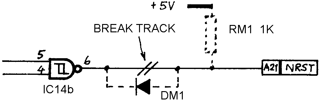
The reason for using Schmitt-trigger gates for IC14 is because the outputs of standard or Low-power-Schottky gates are not guaranteed to be 'clean' if the inputs are fed with slowly changing signals (such as charging capacitors C5 and C6). IC15b has no function in this circuit.4.2.17
Note: According to the ISBUS specification the signal on pin 21 should be open collector (so that when it is '1' some other device (e.g. a simple switch) can reset the system remotely. It would be unduly pedantic to insist on strict adherence to the ISBUS specification on this point but the following circuit shows one expedient method to give the effect of an open collector line:
DM1 in this modification will have to be a germanium type, which has a much lower forward voltage drop than silicon types. Ideally an open collector buffer of some sort should be used but the above modification may be sufficient to get round the problem, if one exists.
4.3 CPU, Power on Jump, Page Decoder Circuit (Page 35)
4.3.1
This circuit shows the CPU chip (IC10) itself. Taking the pins largely in the order they are illustrated on the diagram the various functions are as follows:4.3.2
Pin 6 'ZØ', is the clock input signal which is derived from the circuit already discussed in Section 4.1 above it regulates and defines the speed at which the CPU chip operates.4.3.3
Pins 25, 16, 17 (!BUSREQ, !INT, !NMI) are all tied to a '1' by either R11 or R12. When they are '1' as here, they do not affect CPU operation. An external device would have to take the appropriate line to a '0' to obtain the desired response from the CPU, and the user is referred to the CPU chip data sheets for the description of this response. It is worth mentioning that pins 16 and 25 of IC10 would need to be separated if, as is likely invariably to be the case, individual control of each line was desired. For Mode 2 Interrupt the buffering needs alteration.4.3.4
Pin 26, !RESET , is an input connected to the system NRST line whose action has already been discussed in section 4.2 above. A '0' on this line resets the CPU before operation under program control commences.4.3.5.1
Pin 24 is the '!WAIT' input. When an external device wishes the CPU to wait it takes this line low. A typical example is a simple floppy disc control circuit which would have to ask the CPU to wait until the disc was in just the right position to receive its data. Another example is when the CPU is used with slow memory devices – a wait signal can be produced only by the slow memory address decoder or a crude method is for all memory accesses (fast or slow) to request that the CPU wait for a cycle or two4.3.5.2
In the absence of any such request R13 pulls pin 24 high so that the CPU is not asked to wait unnecessarily. The MZB3 board takes the NWAIT signal to position A30 on the edge connector, but 'ISBUS' board.(To do this cut the track between pads P20 and P21 on the upper (component) surface of the MZB3 board, and use a jumper wire 313 to connect P20 to P25 instead).4.3.6
Pins 13, 10, 9, 7, 8, 12, 15, 14 are the 8 'tristate' data lines. They are bidirectional, and are sometimes inputs and sometimes outputs.4.3.7
Pin 29 is the 0V power supply to the CPU chip.
Pin 11 is the +5V power supply to the CPU chip.4.3.8
Pins 5, 4, 3, 2, 1, 40, 39, 38, 37, 36, 35, 34, 33, 32, 31, 30 are the 16 tristate address lines. They are all outputs. The design of the CPU-chip is such that the address bus is not guaranteed valid before the trailing edge of !ZMREQ on an OP-Code Fetch. The CPU chip manufacturers suggest that a 4 bit latch be used on the top 4 address lines to avoid potentential difficulties in the interface to dynamic RAMs, and IC4, enabled by !ZMREQ provides this function on this board.4.3.9.1
Pin 28 of the CPU is the !RFSH signal output. It goes to a '0' to indicate that the seven lower order bits of the address bus contain a refresh address for dynamic memories.4.3.9.2
The signal if required is taken to edge connector pin A32 'NRFSH', via a jumper wire between circuit board pads P12 and P23.4.5.10
Pin 23 on the CPU chip IC10 is another output: !BUSACK. It goes to a '0' to indicate that the CPU busses are tristate. It is not likely to be used in this application, as the CPU busses are buffered from the edge connector independently.4.3.11
Pins 21 and 22 are the read and write control line outputs. They go low respectively to indicate that the CPU wants to read or write.4.3.12
Pin 27 is the 'machine cycle one’ output. It goes low to indicate the CPU is currently fetching an operation code (OP-code). Its main use here is for synchronisation purposes, e.g. for the reset circuitry described in section 4.2.4.3.13
Pins 19 and 20 on IC10 are the 'Memory Request’ and 'I/!O Request' output signals which are buffered and used by the system. A ’0' indicates that the address and data on the bus are associated with either the Memory or the Input/Output Ports, according to which line is '0'.4.3.14.1
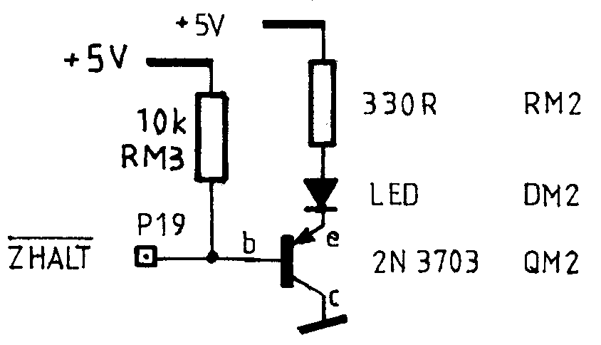
Pin 18 is a '!HALT' output which goes to a ’0' to indicate that the CPU has just executed a 'HALT' instruction and is waiting for an interrupt input in order to continue. The signal can be used for various purposes, but if a visible indicator is required the following circuit can be used and built up in any convenient manner:
(QM2 is an emitter follower, which amplifies the current the CPU can sink into pin 18, to allow about 10mA (limited by RM2) to flow in LED DM2).
4.3.15.1
The PJUMP signal will be described in Section 4.4 but for the moment it can be taken that at 'power-on' it is at a '1'. The top 4 address lines, (which have been latched by !ZMREQ in the manner already described) are the Q output pins 16, 15, l0, 9 or IC4 and a suitable combination of links, as listed in the 'Table of Jump Addresses' given on the diagram, will cause the 4 addresses JA15, JA14, JA13, JA12 to be set to any chosen 4K page. The method of operation is as follows:4.3.15.2
At 'power-on' the CPU issues an address on page 0 and so the 4 outputs of IC4 are all '0'. If the program in the system begins on page 0 then JA15, JA14, JA13 and JA12 should all be ’0' and so jumper links J2, J6, J4 and J8 should all be made. (In this case IC5 will be serving no purpose - the output of an 'OR' gate with '0’ an both inputs is '0', and '1' if the inputs are '1') 4.3.15.3 However, if for some special purpose it is wished to locate the program on some other 4K page, then the links J1 to J8 can be rearranged to route the '1' from the PJUMP line into one or more of IC5's inputs and jam the address outputs to any chosen page. The Ths table of address gives details of the specific jumper links to be inserted, but the basic principle is that if the output line is to be '0' the two 'OR' gate inputs are joined together to the appropriate IC4 Q output, and if' a '1' is required, one of the 'OR' gate inputs is connected instead to the 'PJUMP' line.4.3.15.4
(Of course, for a fixed page '0' it might be more convenient simply to remove IC5 and link pins 2-3, 12-11, 5-6, and 9-8 fitting none of links J1-J8).4.3.15.5
Under software control PJUMP is usually returned to '0' at some stage and so the effect of the Jump address links is cancelled and JA15, 14, 13, 12 are then the same as the addresses A15, 14, 13, 12 issued by the CPU.4.3.15.6
(The reason the power-on-jump feature is incorporated is to use the CPM floppy-disc operating system which requires RAM, not ROM, on page 0. In such a system all the programs are stored on magnetic discs, and transferred to the computer's RAM before they are run. This means there is no need for any ROM in the system, except for the tiny program, which first loads the computer from disc.)4.3.16.1
This ROM is called a 'Boot ROM’ and is IC11 on this board. It obviously cannot reside on page 0 while loading RAM which is also at the same addresses, hence the necessity of a power-on-jump to some other clear address).4.3.16.2
The remaining part of this circuit is the page decoder IC6. One of four links T1 - T4 one of four links T5 - T8 are inserted according to the table provided on the diagram and these select the address of IC11, the on-board PROM. the top four address lines (J12, J13, J14, J15) are the inputs to IC6 and the selected page output SEL will go low when 312 - 15 correspond to the chosen page, as selected by links T1 - T8. Links T1-T8 are single hole through ('thro') links which connect one side of the board to the other, so care should be taken to ensure no connection remains if a link is changed to another position.4.3.16.3
The type of memory selected for the 'Boot PROM' IC11 is usually 1K or 2K and yet !SEL covers an entire 4K page. Therefore no other device than IC11 can be located on the chosen page. This is generally of little consequence for a 'Boot PROM' as it remains in circuit only long enough to load the operating system into RAM from the floppy disc - it is then switched out of circuit leaving the whole SEL page clear for e.g. RAM.
4.4 The diagram on page 36 shows the 'Boot PROM'
IC11
and some associated circuitry.
4.4.1
After the reset pulse, '!RST' is over, the positive edge where it returns from '0' to '1' is used as a clock pulse for IC2a and IC2b (top left hand corner of the diagram. As the '0' inputs (pins 2 and 12) of IC2a and IC2b are both '1' this causes output Q (pin 5) 'PJUMP' to be '1' and output Q (pin 8) to be '0'. The 'PJUMP' output has already been discussed in section 4.3, and it is used to produce a chosen 'power-on-jump' to a chosen page.4.4.2
The '0' output on pin 8 of IC2b is used to enable the on-board boot PROM, IC11. There are three inputs to the NOR-gate IC3a and at this stage IC3a, pin 2 is '0' because it is connected to pin 8 of IC2b. To read the boot PROM the CPU will have made !ZRD a '0', and the issued address (modified by the power-on-jump circuit) will cause SEL also to be a '0'. This pin 1 of IC3a will be '0' because it is connected to !ZRD, pin 13 will be 0 because !SEL is '0' and pin 2 is already '0'.4.4.3
All '0's on the input to a NOR gate is the sole condition which causes its output, in this case pin 12 of IC3a to go to a '1'. Thus !BUFFEN is '1' !BUFFEN will be mentioned again in section 4.5 below but for the moment we shall simply say the !BUFFEN = 1 is the condition which divorces the system data lines from the CPU data bus leaving them free to be controlled by the 'boot PROM' IC11.4.4.4
The '1' on IC3a pin 12 is inverted to '0' by IC3b and this '0' is used to select IC11 via the chip select input pin 20 at IC11. Thus only the data from the on-board PROM IC11 at its power-on-jump address reaches the CPU.4.4.5
When other addresses are isssued by the CPU !SEL goes to a '1', and when the CPU is writing to memory !ZRD is '1'. In these cases either or both pins 13 and 1 of IC3a are '1' and the output pin 12 is '0'. This '0' on the !BUFFEN line enables the data buffer so that the CPU has access to and from the system-data bus. The inverter-connected IC3b inverts the '0' to a '1' and so pin 20 of IC11 is high, effectively switching it out of the circuit.4.4.6
As mentioned in Sections 3.5 and 3.6, the main purpose of IC11 is to be a 'boot PROM' in a floppy disc system, and once it has completed its brief but all important task, the power-on-jump line PJUMP should be returned to '0' and the boot PROM should be switched permanently out. This is achieved in two stages under software control as follows:4.4.7
Firstly a 'READ FROM OUTPUT PORT FF' CPU instruction is executed. This causes the eight address lines ZA0-ZA7 to go to all '1's (since 'FF' = all ''1's), !ZI/0 goes to a '0' to indicate an I/0 request, and !ZRD goes to low for a read. The eight '1's on the inputs of IC12 are 'NANDED' to make output pin 8 of IC12 a '0'. The two '0's on pins 1 and 2 or ICla leave output pin 3 as a '0' and the two '0' on pins 9 and 10 of IClc result in a '0' on pin 1 of IC2a which resets it to '0', thus making PJUMP'0' and re-moving the power-on jump.4.4.8
Secondly a 'WRITE TO OUTPUT PORT FF' CPU instruction is executed. As in the previous paragraph, output pin 3 of IC1a is '0' and therefore so is pin 12 of IC1d. !ZWR is '0' for a write and this is connected to pin 13, the other input of IC1d. The output pin 11 of IC1d is '0' and thus IC2b gets reset: Q, pin 8 of IC2b, is one of the inputs of IC3a, and is now fixed at '1'. A '1' on any input of a 'NOR-gate'(IC3a) causes an output '0' regardless of the state of the other inputs, !SEL pin 13 and !ZRD pin 1.4.4.9
Henceforth PJUMP is '0', removing the power-on-jump address, !BUFFEN is '0' permanently enabling the 8-bit system data buffer, and !CS pin 20 of IC11 is '1' permanently deselecting it.4.4.10
IC11 can be either a 2516 or 2708 type of EPROM. If cost can be disregarded the best device is the 2516, since it is easy to program and requires only a single 5V supply. Although the 2708 device is cheaper it has the disadvantage that it needs additional supply voltages +12V, and -5V. Although +12V is a standard 'ISBUS' power rail, -5V is not, and so -5V has to be derived from the -12V standard 'ISBUS' power rail. Fortunately a simple series-connected 6.8V Zener diode will drop approximately 7 volts and the -5V supply for the 2708 is quite simply obtained from the standard 12V.4.4.11
The appropriate changes are given in the notes at the top right hand side of the diagram on page 36 . It is vital to get these connections absolutely correct, as a wrong connection in this area is almost certain to cause damage.4.4.12
The 2708 type of EPROM consumes about 40 mA and so the dissipation in the 6.8V Zener is fairly large at about 280 mW. This is why the technique is not used where several 2708s are involved, and a proper -12V to -5V regulator is used instead.4.4.13
Of course if the user wishes to deviate from the ISBUS standards, it is perfectly possible to supply -5V to the edge connector pins A38 and A39, in which case no track cutting or Zener Diode is necessary.
4.4.14
IClb and IC3c are not used in this circuit and so are available for any special purposes the user may have.4.5.1
The circuit of the buffers (page 37) needs hardly any explanation. ICs 7, 8, 13 are standard non-inverting buffers which buffer the named signals. They are permanently enabled by having their 'Enable' pins !E1 and !E2 connected to '0'. Because both enable pins are at '0' it is possible to substitute different devices in a case of supply difficulty. The alternative types are named on this diagram.4. 5. 2
IC17 is an octal bi-directional transceiver. Pin 19 is the single enable input E, connected to the !BUFFEN line which has already been discussed in section 4.4.4.5.3
When !BUFFEN is '1' both sides of IC17 are tristate,but when it is '0' one or other of the two 8-bit sides is connected to the other side. The direction is controlled by the !ZRD signal, connected to pin 1 of IC17.4.5.4
When !ZRD is '0' (i.e. the CPU is wishing to 'read' the data on the system data bus DB0 - DB7), the direction is from the 'B' side to the 'A' side of IC17, that is from DB0-7 to ZD0-7. When the CPU is 'writing' to the system data bus !ZRD is '1', and in this case the direction is from the 'A' side to the 'B' side i.e. from ZD0-7 to DB0-7.4.5.5
For special applications it may be desired to 'tristate' the bus and effectively isolate the board from the system. This is simply achieved in ICs 7, 8, 13 by taking their respective '!Enable' lines to a '1'. IC17 presents more of a problem: either pin 19 must be forced to an unconditional '1' or the direction must be permanently reversed by presenting an unconditional '0' to pin 1. It is likely some of the spare gates e.g. IClb, IC3c, IC9f can be used to advantage to achieve this.
4.6 Power Supply and Decoupling Capacitors (Page 38)
4.6.1
This is the remaining section of the circuit diagram. It is mainly for reference purposes, for example when testing or fault finding. Some of the symbols used on the diagrams are explained and the various power supply connections and decoupling capacitors are identified.4.6.2
Although the power supply connections are largely irrelevant to logic diagrams, as are the decoupling capacitors and therefore often left off such diagrams, they nevertheless represent invaluable information when fault finding.4.6.3 Both options for IC11 have been listed, and both ends of the capacitors (in common with all the resistors and capacitors on all the diagrams) have been numbered 1 and 2, to help during testing.
4.6.4.1 Except for R1 (top left hand corner of diagram on page 36 ), all TTL '1's have been connected directly to the +5V rail, without a limiting resistor.
4.6.4.2 There is a school of thought that says a limiting resistor should be included when connecting a TTL, or LSTTL etc., input to the +5V line. TTL inputs are connected to the emitter of a base-emitter junction which breaks down at about 9 volts, the action being similar to a Zener diode, and the resistor is included to keep the current down to a few mA to prevent permanent damage. See correction below. *
4.6.4.3 Kemitron's argument in leaving this component out is that the +5V line should never rise to +9V in any circumstances, and with modern crowbar protected power supplies there is a lot of truth in this statement. Certainly actual operating experience confirms that damage due to this cause is unlikely. We have heard of an isolated case of unexplained damage to a computer, but this was reported to have taken place during a thunderstorm, and it is debatable whether any measures can be taken to provide protection against lightning strikes! See correction below. *