Color Computer Technical Reference Manual
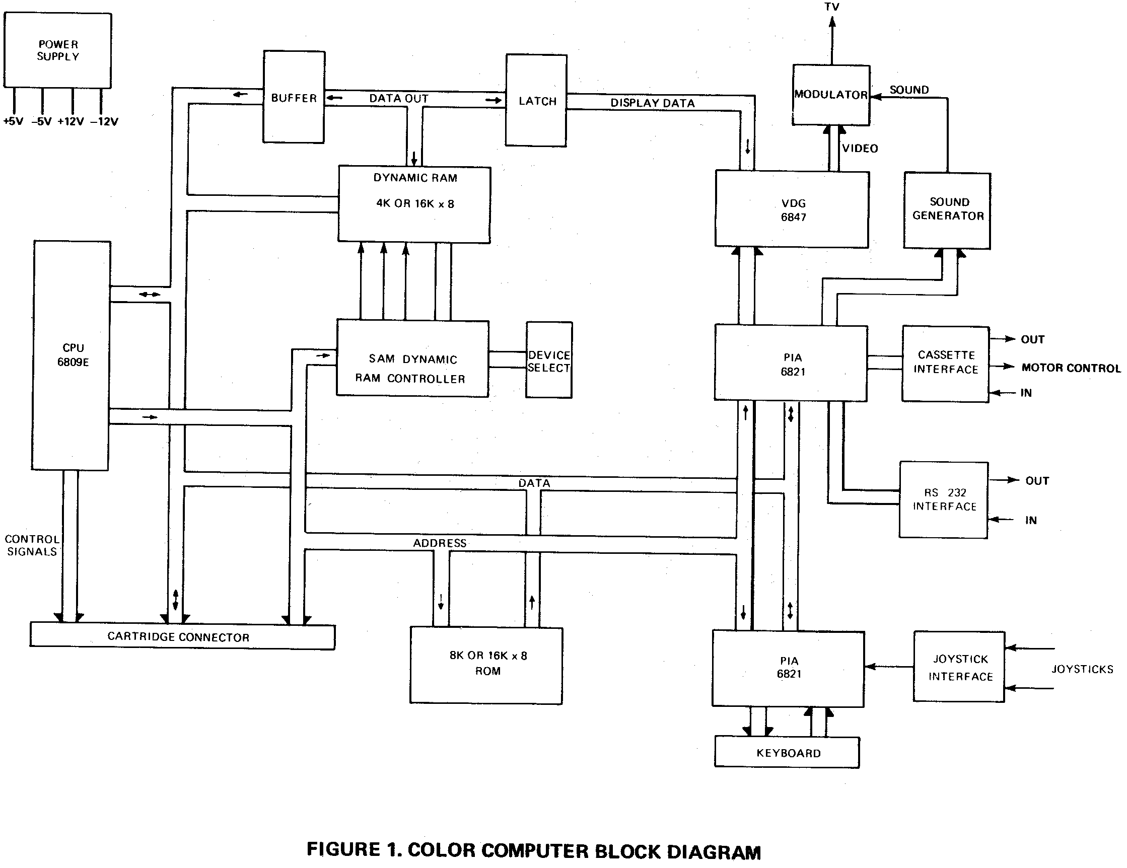
The primary functions of the Color Computer are performed by five 40-pin Large Scale Integration (LSI) chips plus Random Access Memory (RAM) and Read Only Memory (ROM). These five chips are indicated on the Block Diagram (Figure 1) by CPU, SAM, VDG, and two PIA's. With only these five chips plus RAM, ROM, and a power supply, the Color Computer would operate and provide a composite video output. However, to allow communication with the outside world, I/O interfaces must be added.
The main component of any computer system is the Central Processor Unit (CPU). It is the duty of the CPU to provide or request data and select the proper address for this data. In addition, the CPU is capable of performing a limited set of mathematical and logical operations on the data.
ROM has the duty of providing the CPU with a predefined set of instructions. Without ROM, the CPU would run wild and randomly execute instructions. In normal operation, the CPU jumps to the start address in ROM after the reset switch has been pressed, and then performs the reset program to set up all of the programmable devices. Following this, the BASIC instruction set residing in ROM is in control of the CPU.
RAM provides storage for the programs and/or data currently being executed. In addition, this same RAM is used to generate the video display. Normally, no conflict will be observed because the program will use one portion of RAM and the display will use another. During normal usage, the BASIC interpreter located in ROM will control the execution of programs located in RAM.
A central component in the Color Computer is the dynamic RAM controller chip (SAM). This chip provides refresh and address multiplexing for the RAM. It also provides all of the system timing and device selection.
The video display generator (VDG) provides virtually the entire video interface on one chip, and allows several different alphanumeric and graphic modes. This mode of operation of the VDG is controlled by one of two peripheral interface adapters (PIA's) used in the Color Computer. With this information and RAM data, the VDG generates composite video and color information for the modulator circuitry.
The remaining circuitry in the Color Computer is devoted to Input/Output (I/O) communication. The most important part of this circuitry is the keyboard which allows the operator to enter information. Other I/O circuits are provided to allow joystick inputs, cassette input and output, and RS232 input and output.
Figure 1: System block diagram
The first page of the Memory Map (page 5) shows the break-down of the large blocks of memory in the Color Computer. One variable in this block is the video display which may be located anywhere in the memory. BASIC normally locates the video display at the hexadecimal addresses 0400 - 05FF.
The next two pages of the Map explain the addressing for the PIA's. In general, the even numbered memory locations are the I/O registers and the odd numbered memory locations are the control registers. Bit two of the control registers determines what is addressed at the even numbered memory locations. If this bit is set high (logic 1) the data I/O register is addressed. If it is set low the data direction register is addressed. Normally the data direction register is addressed only during initialization to allow configuration of the data inputs and outputs. (By clearing bit 2 and writing to the even numbered memory location one address below, each bit of the PIA may be set as an input or an output. A 1 in the data direction register sets the bit as an output and a 0 sets the bit as an input.)
The addresses from FFC0-FFDF are the control registers for the SAM address multiplexer chip. There are no data lines to the SAM chip therefore two addresses are used to control each register. In general, writing any data to an even numbered memory location will clear the register and writing any data to an odd numbered memory location will set the register. Addresses FFC0-FFC5 control the display mode. To select a certain display mode, both these registers and the PIA controlling the VDG chip must be set to the proper mode. However, it is also possible to set the SAM registers to one mode and the PIA controlling the VDG to another mode, and obtain a useful video mode. These cross modes are explained in more detail in the Video Interface section.
However, it is also possible to set the SAM registers to one mode and the PIA controlling the VDG to another mode, and obtain a useful video mode. These cross modes will be discussed in more detail in the Video Interface section.
Addresses FFC6-FFD3 control the display starting address. If all of the registers are cleared, the display will begin at 0000. Normally register F2 will be set causing the display to start at 0400. This feature of the SAM chip allows the display to be paged through all of the RAM. Register P1 controls a feature which is not used in the Color Computer. Therefore, it should be cleared at all times.
Addresses FFD6-FFD9 control the clock speed of the CPU. The Color Computer is designed to operate at 0.89 MHz.
Addresses FFDA-FFDD control the memory size set up of the SAM chip. These addresses select 4K, 16K, or 32K of RAM in the Color Computer. This memory size option should be changed only by the reset routine in BASIC. Changes at other times may erase the contents of RAM. Register TY, at addresses FFDE - FFDF, should be cleared at all times.
The final series of addresses in the Color Computer are the interrupt and reset vectors. Whenever the CPU receives a reset or interrupt it will load the address at the indicated location and begin execution at the new location. The dual set of addresses are listed because the vectors are mapped into the top of the BASIC ROM (BFF2-BFFF), i.e., if the CPU reads FFFF it will actually read the contents of BFFF.
| Range | Size | CoCo | ||
| 0000-0FFF | 4K | 16K | 32K | RAM 0400-05FF = |
| 1000-1FFF | ||||
| 2000 3000 |
||||
| 4000 5000 |
||||
| 6000 7000-7FFF |
||||
| 8000 9000-9FFF |
8K | Extended Color BASIC ROM |
||
| A000-AFFF B000-BFFF |
8K-256 * | Color BASIC ROM | ||
| C000-CFFF D000-DFFF |
8K | Cartridge expansion |
||
| E000-FEFF | 8K-256 * | |||
* The last 256 bytes of these ROM spaces contain the I/O locations and the reset vectors
| FF00-FF03 | 4 | 6821 PIA 0 | FF00 | |
| FF00 | ||||
| FF00 | ||||
| FF03 | ||||
| FF04-FF07 | NOT USED | |||
| FF08-FF1F | NOT USED | |||
| FF20-FF23 | 4 | 6821 PIA 1 | FF20 | |
| FF21 | ||||
| FF22 | ||||
| FF23 | ||||
| FF24-FF3F | ||||
| FF40-FF48 | 8 | NOT USED |
| FFC0-FFDF | 32 | 6883 SAM | FFC0 | C | V0 |
|
||||||||||||||||||
| FFC1 | S | |||||||||||||||||||||||
| FFC2 | C | V1 | ||||||||||||||||||||||
| FFC3 | S | |||||||||||||||||||||||
| FFC4 | C | V2 | ||||||||||||||||||||||
| FFC5 | S | |||||||||||||||||||||||
| FFC6 | C | F0 | Display
offset (binary) Address of
upper-left-most |
|||||||||||||||||||||
| FFC7 | S | |||||||||||||||||||||||
| FFC8 | C | F1 | ||||||||||||||||||||||
| FFC9 | S | |||||||||||||||||||||||
| FFCA | C | F2 | ||||||||||||||||||||||
| FFCB | S | |||||||||||||||||||||||
| FFCC | C | F3 | ||||||||||||||||||||||
| FFCD | S | |||||||||||||||||||||||
| FFCE | C | F4 | ||||||||||||||||||||||
| FFCF | S | |||||||||||||||||||||||
| FFD0 | C | F5 | ||||||||||||||||||||||
| FFD1 | S | |||||||||||||||||||||||
| FFD2 | C | F6 | ||||||||||||||||||||||
| FFD3 | S | |||||||||||||||||||||||
| FFD4 | C | P1 | Page number (=0) | |||||||||||||||||||||
| FFD5 | S | |||||||||||||||||||||||
| FFD6 | C | R0 |
|
|||||||||||||||||||||
| FFD7 | S | |||||||||||||||||||||||
| FFD8 | C | R1 | ||||||||||||||||||||||
| FFD9 | S | |||||||||||||||||||||||
| FFDA | C | M0 |
|
|||||||||||||||||||||
| FFDB | S | |||||||||||||||||||||||
| FFDC | C | M1 | ||||||||||||||||||||||
| FFDD | S | |||||||||||||||||||||||
| FFDE | C | TY | Map Type | |||||||||||||||||||||
| FFDF | S |
| Address | Contents | |
| FFF1 to FFE0 | NOT USED | |
| FFF0 or BFF0 | MSB | NOT USED |
| FFF1 or BFF1 | LSB | |
| FFF2 or BFF2 | MSB | SWI3 VECTOR |
| FFF3 or BFF3 | LSB | |
| FFF4 or BFF4 | MSB | SWI2 VECTOR |
| FFF5 or BFF5 | LSB | |
| FFF6 or BFF6 | MSB | FIRQ VECTOR |
| FFF7 or BFF7 | LSB | |
| FFF8 or BFF8 | MSB | IRQ VECTOR |
| FFF9 or BFF9 | LSB | |
| FFFA or BFFA | MSB | SWI1 VECTOR |
| FFFB or BFFB | LSB | |
| FFFC or BFFC | MSB | NMI VECTOR |
| FFFD or BFFD | LSB | |
| FFFE or BFFE | MSB | RESET VECTOR |
| FFFF or BFFF | LSB | |