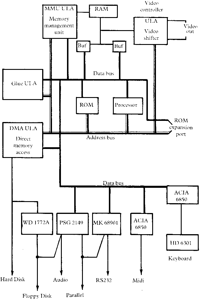
The Atari ST computer system consists of a console unit featuring an integral keyboard, a display screen, sound subsystem, peripheral input/output and an operating system. Expansion ports are provided for the connection of a variety of peripheral devices i.e. a mouse, joystick, printer, modem, floppy disk, ROM cartridge application program etc.
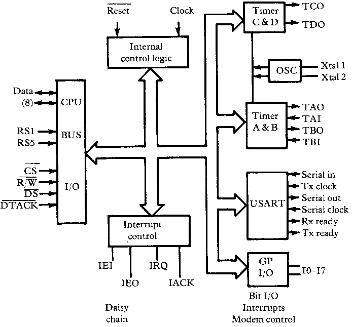
The Atari ST console contains an 8MHz MC68000 16 bit microprocessor, at least 512K of resident RAM and a 192K ROM operating system. A Mostek MK68901 multi function peripheral (MFP) device provides the general purpose interrupt control and timers and a single direct main memory access channel, giving both high and low speed access support, through a 32-bit FIFO to the 8 bit device controllers.
User input is via the integral intelligent keyboard, an external mechanical and or optical mouse, or a switch type joystick. The keyboard communicates bidirectionally at 7 Kbits/s with the main unit via a 1MHz HD6301 8-bit microprocessor in the keyboard unit, and a MC6850 asynchronous communications interface adapter (ACIA) in the ST console.
The display may be either a monitor, high resolution black and white or colour (The Atari STM also caters for a standard television display unit). The console interrogates the display device to determine the type attached, ensuring the high frequency sync signals are not sent to low frequency monitors. There are three display resolutions, 320 x 200 16-colour low resolution, 640 x 200 4-colour medium resolution and 640 x 400 high resolution monochrome. The display memory is part of the main memory and provides a matching bit-pixel relationship to the physical screen in high resolution mode, with the screen origin at 0,0 in the top left hand corner being bit 15 of word 0. The monochrome monitor (SM124) is capable of a high quality display of the high resolution 640 x 400 ST graphics.
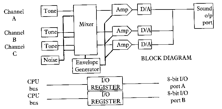
The music system sound effects and audio feedback output are created through the monitor or television speaker, at frequencies in the range of 30Hz to 128Khz, via three independent voice channels. The programmable sound generator outputs may consist of a noise and a tone mixed at a fixed or variable amplitude defined by the envelope generator.
The musical instruments digital interface (MIDI) enables the ST to integrate with music synthesisers, sequencers, drum boxes etc. which incorporate the MIDI interface; enabling OMNI, POLY and MONO networking.
Printer output is achieved via the parallel or RS232 interfaces, the latter also being available for modem and general communication.
The floppy and hard disk interfaces provide the off-line data and program mass storage facilities, the hard disk drive interface being accessed through the DMA controller. An on-board Western Digital WD1772A supplies the floppy disk drive controller which interfaces the Atari ST 3.5" disk drives (SF354 or SF314).
| MONITOR RGB composite |
PLUG-IN CARTRIDGE 128K
ROM max |
FLOPPY DISK 349 Kbytes formatted |
| DMA PORT Direct
|
MAIN SYSTEM 8
MHz 68000 processor Graphics subsystem: 32k bit map Sound subsystem: Programmable ROM 192K Packages: MC 6850 |
FLOPPY DISK INTERFACE Supports two drives WD1772A |
| PARALLEL PRINTER INTERFACE Centronics MC 68901 |
RS232 I/F rts/dtr/cts/dcd/ring MC 68901 |
|
| MIDI I/F Omni-Poly
|
||
| INTELLIGENT KEYBOARD HD 6301 |
MOUSE/JOYSTICK PORT Two-button mouse |
|
| JOYSTICK PORT | ||
The operating system may be either in 192K of ROM, or an image file on disk loaded by the disk's boot sector, featuring the GEM operating environment of windows, icons, pull-down menus. The ST is also supplied with two language implementations, an interpreted BASIC and Atari LOGO.
The ST can accept other operating systems loaded via the boot sector or brought up by a driver in an 'auto' folder.
 |
Power 7 way DIN7S (if external) |
 |
MIDI out 5 way DIN5S socket |
|
MIDI in 5 way DIN5S socket |
 |
Video RCA pin jack (if fitted) |
 |
Monitor
output composite and RGB 13 way DIN13S socket |
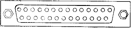 |
Parallel
8-bit bidirectional printer port 25 way DB25S socket |
|
RS232 modem
port 25 way DB25P plug |
 |
Floppy disk
controller 14 way DIN14S socket |
 |
Hard disk
DMA port 19 way DB19S socket |
 |
ROM
expansion port 40 way socket |
 |
Joystick 9 way DB9P plug |
|
Joystick
(configured as a mouse) 9 way DB9P plug |
| Monochrome monitor Atari
SM124 Colour monitor Atari SM1224 RGB |
Television
(where fitted) RCA
pin jack |
|
13 way
DIN13S socket Sync 5V active low 3.3
kilohm |
| Pin | Function | ST signal processing device |
| 1 | Audio out | |
| 2 | Composite video | |
| 3 | General purpose output | TTL PSG I/O A |
| 4 | Monochrome detect, active low, 1K pull-up to 5V | TTL MFP |
| 5 | Audio in | |
| 6 | Green | |
| 7 | Red | |
| 8 | Ground | |
| 9 | Horizontal sync | |
| 10 | Blue | |
| 11 | Monochrome | |
| 12 | Vertical sync | |
| 13 | Ground | |
The monitor output supports either a high resolution black and white monitor (Atari SM124) or a medium resolution colour monitor (Atari SC1224). Sound is reproduced through the display device speaker.
Any suitable monitor may be attached, typical performance:
| Low | Medium | High | |
| Resolution | Resolution | Resolution | |
| Resolution | 452 x 585 pixels | 653 x 585 pixels | 895 x 585 pixels |
| Video Bandwidth | 10 MHz | 18 MHz | 18 MHz |
| Slot pitch (typ) | 0.64 mm | 0.41 mm | 0.31 mm |
| Vertical scan | 50/60 Hz | 50/60 Hz | 71.2 Hz |
| Input video | 1 VDC pk-pk | ||
| Input audio | 1 VDC pk-pk | ||
| Sync | 5 VDC active low | ||
| MFP | <-- | 11 | Busy | ||
| PSG | I/O port B | ==> | 2...9 | Data | |
| I/O port A bit 5 | --> | 1 | !Strobe | ||
| main console | I/O port | ||||
The parallel port interface provides an 8-bit data communication channel controlled by a strobe signal generated by the ST, indicating that data bits are available on the data lines for transfer to the peripheral, and a busy signal generated by the peripheral (usually a printer) indicating either that it is busy, has a fault or possibly out of paper if a printer.
25 way DB25S socket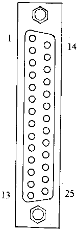 |
|
The parallel port strobe signal generated by the PSG I/O port A (pin 1), supplies the data transfer synnchronization.
The busy signal (pin 11) is read by the console MFP and provides the handshake control.
The strobe signal is active low, the busy signal active high, with a 1Kohm pull-up resistor to + 5V. All signals are at TTL levels.
| MFP | --> | 2 | TX | transmit | ||
| <-- | 3 | RX | receive | |||
| <-- | 5 | CTS | clear to send | |||
| <-- | 8 | DCD | data carrier detect | |||
| <-- | 22 | RI | ring indicator | |||
| PSG
write-only I/O port A (FF8802) |
bit 3 | --> | 4 | RTS | ready to send | |
| bit 4 | --> | 20 | DTR | data terminal ready | ||
| main console | I/O port | |||||
The RS232 interface is controlled via the PSG I/O port A (RTS and DTR) and the MFP (CTS, DCD and RI) transmitting and receiving data within the range 50 to 192K baud, the timing synchronization is generated by the multi-function processor (MFP) timer D.
The interface supports hardware handshake control:
| Transmit PSG I/O port A | Receive MFP inputs | Software control is through Xon/off protocol. |
| RTS | CTS Ring | |
| DTR | DCD |
25 way DB25P plug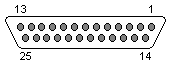 |
|
|||||||||||||||||||||||||||||||||||||||||||||
RS232 signal levelsZero +3V to +12V One -3V to -12V |
||||||||||||||||||||||||||||||||||||||||||||||
| WD1772A | --- | 4 | index pulse | |
| --> | 8 | motor on | ||
| --> | 9 | direction in | ||
| --> | 10 | step | ||
| --> | 12 | write gate | ||
| PSG | --> | 2 | select side | |
| --> | 5 | drive 0 | ||
| 6 | drive 1 | |||
| main console | I/O port | |||
The floppy disk interface is based on an on-board Western Digital WD1772A disk controller and supports a maximum of two drives. There is no hardware sensing of disk removal. The drives provide fast storage and retrieval of data and programs on 3.5” flexible micro disks.
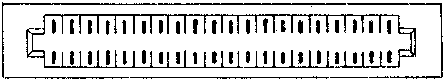
14 way
DIN 14S socket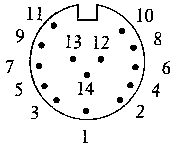 |
|
Data is written to 512 byte sectors.
This port can be use to provide access to a hard disk or a compact disk. The hard disk controller communicates through a sequence of six bytes which provide format, read and write facilities etc. The command protocol used is referred to as ANSI X3T9.2, a SCSI-like small computer systems interface, of which the ST supports a small subset.
The Atari hard disk descriptor block consists of a six byte command packet conforming to the following:
Six byte command packet
Byte
No/Bit
No.Function Range 0 0-4 Operation code 0-31 5-7 Controller number 0-7 1 0-4 Head number. 5-7 Cylinder number high 2 0-5 Sector number 0-63 6-7 Drive number 0-7 0-31 3 0-7 Cylinder number low 4 0-7 Sector count 5-7 0-7 Control byte
Hard disk command code summary
Op code Command Dec Hex 5 05 Verify track Multi-sector transfer with implied seek 6 06 Format track 8 08 Read sector 10 0A Write sector 11 0B Seek 13 0D Correction pattern 26 1A Mode sense
There is only one DMA channel which is shared by both high- (up to 8 Mbit/s) and low- (250 to 500 kbit/s) speed 8-bit device controllers.
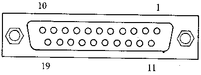
19 way DB 19S socket
Pin Function Signal type 1 data 0 TTL 2 data 1 3 data 2 4 data 3 5 data 4 6 data 5 7 data 6 8 data 7 9 chip select TTL active low 10 interrupt request TTL active low, 1K pull up 11 ground 12 reset TTL active low (system reset) 13 ground 14 acknowledge TTL active low 15 ground 16 A1 TTL 17 ground 18 read/write TTL 19 data request TTL active low, 1K pull up
| ACIA | --- | Rx receive data | ||
| --> | Return |
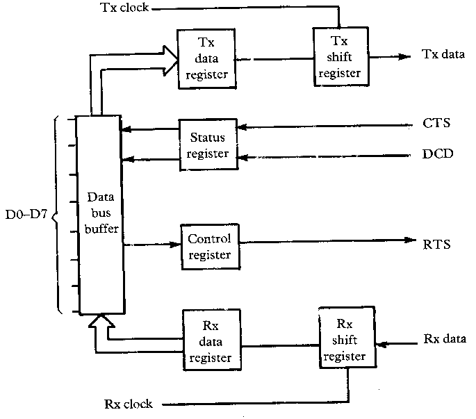
The MIDI interface functions through an MC6850 asynchronous communications interface adapter ACACIA) whose control/status register is located at $FFFC04 (16776196); data is passed in the register at offset 2 from the control / status register.
Data is transmitted serially via the MIDI ports through 2 pins asynchronously using the protocol:
|
|
The MIDI OUT port also supports the optional through port which merely provides the MIDI IN signals through an opto-coupled isolator at the MIDI OUT connector.
Control of the port is available through the ST’s extended BIOS.
| MIDI in | MIDI out/through |
5 way DIN 5S socket  |
5 way DIN 5S socket |
Pin Function 1 n.c 2 n.c 3 n.c 4 In receive data 5 In loop return |
Pin Function 1 Through transmit data 2 Shield ground 3 Through loop return 4 Out transmit data 5 Out loop return |
The MIDI ports may be used to network data between connected computers.
This port provides a plug-in cartridge facility that does not sense in hardware the presence of a cartridge. The cartridge ROM occupies addresses in the range: $FA0000 (16384000 ) to $FBFFFF (16515071) – maximum 128 Kbytes
40 way 40S socket
| function | pin | function | ||
| power + 5 VDC | 2 | 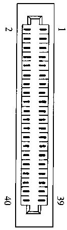 |
1 | power + 5 VDC |
| data 15 | 4 | 3 | data 14 | |
| data 13 | 6 | 5 | data 12 | |
| data 11 | 8 | 7 | data 10 | |
| data 9 | 10 | 9 | data 8 | |
| data 7 | 12 | 11 | data 6 | |
| data 5 | 14 | 13 | data 4 | |
| data 3 | 16 | 15 | data 2 | |
| data 1 | 18 | 17 | data 0 | |
| address 15 | 20 | 19 | address 13 | |
| address 14 | 22 | 21 | address 8 | |
| address 9 | 24 | 23 | address 7 | |
| address 10 | 26 | 25 | address 6 | |
| address 12 | 28 | 27 | address 5 | |
| address 4 | 30 | 29 | address 11 | |
| address 3 | 32 | 31 | ROM3 select | |
| address 2 | 34 | 33 | ROM4 select | |
| address 1 | 36 | 35 | upper data strobe | |
| ground | 38 | 37 | lower data strobe | |
| ground | 40 | 39 | ground | |
Only the lower 15 address lines are available to the ROM cartridge which does not provide a ‘write’ line.
The Atari intelligent keyboard performs a variety of functions that include the decoding of the key switch matrix, decoding mouse, trackerball and joystick data and providing the time of day. It communicates with the main processor over a high speed bi-directional serial link providing a convenient mouse/joystick interface.
The keyboard consists of a series of make/break key switches for which the ikbd generates keyboard scan codes for each key press and release, chosen mainly for compatibility with the Digital Research graphic system (GSX). The key codes (see table in appendix D) are defined for the whole range of international keyboards such that each code has a predefined key press meaning, irrespective of the presence of the key switch. The break code for each key is signified by bit 7 of the corresponding make code for the key being set; the codes #$F6 to #$FF are reserved for keyboard system functions.
The keyboard controller contains a 1 MHz HD6301 8-bit microprocessor that communicates with the ST’s MC6850 asynchronous communications interface adaptor (ACIA) at a fixed 7.8 Kbit/s. The keyboard not only transmits the encoded key scan codes (with a two key rollover), it also enables the programmer to interrogate the status, define the read rates and sensitivity of the mouse and joysticks under software control.
The time-of-day clock incorporated in the keyboard controller is held to a resolution of 1 second and may be read and set from software. The keyboard may be reset, without affecting the time held by the clock, to its power-up parameters.
When reset, the keyboard controller performs a simple ROM (checksum), a series of RAM and key (stuck) checks, correct operation is indicated by the return of the version/release number of the ikbd controller.
The mouse and joysticks work on the basic unit of an ‘event’, this is defined as either the opening or closing of a switch, or of motion beyond a predefined programmable threshold level. The mouse is capable of a resolution of 200 events per inch (4 events/mm) and is scanned at such a rate as to permit tracking velocities of up to 10 inches per second (250mm/s), at a maximum pulse phase error of 50%.
Motion, which produces make then break cursor keycodes, can be reported in three different ways: relative, absolute and cursor key motion (motion per keystroke is independently programmable in both axes). The mouse buttons can also be treated as part of the mouse or as additional keyboard keys.
9 way
DB9P plug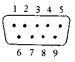 |
Port 0 is configured for mouse
operation Port 1 is the second joystick interface |
||||||||||||||||||||||||||||||
|
|||||||||||||||||||||||||||||||
The mouse unit provides interactive input to programs like the desktop applications, permitting a convenient method of selecting from a menu of facilities shown symbolically as icons or simply as text. Port zero is configured for the mouse, but may also be connected to a joystick.
The joystick is invariably used in games applications; but may also be used instead of the cursor keys, for fine control of the screen cursor position (one pixel movement).
The joystick fire and mouse buttons close to ground.
The power supply provides power for the main system board, the keyboard controller, any connected expansion ROM and expansion RAM.
The supply is fused, the levels are regulated for over-voltage and incorporate over-current protection.
7 way DIN 7P plug
Pin Function
1   +5 VDC
2   n.c.
3   Ground
4   +12VDC
5   -12 VDC
6   +5 VDC
7   Ground
Power levels:
 +5 VDC @ 3A     5%
+12 VDC @ 0.03A 10%
-12 VDC @ 0.03A 10%
The power supply may be integral with the main unit.
MC68000 8 MHz microprocessor
WD1772A floppy disk controller
MK68901 multi-function processor
MC6850 asynchronous communications interface adaptor
YM2149 programmable sound generator
Custom designed devices (ULAs):
Direct memory access controller (DMA)
Memory management unit (MMU)
Video controller (Shifter)
General housekeeping (Glue)
Signal I/O
The following is a very brief description of the signal I/O of the Motorola MC68000.
| VCC | -MC68000- | A0 to A23 |
Address bus --> | |||
| GND | ||||||
| CLK | ||||||
| Processor status |
FC0 | D0 to D15 |
<-- Data bus --> | |||
| FC1 | ||||||
| FC2 | ||||||
| Synchronous control |
!AS | !DTACK | Asynchronous
control |
|||
| !UDS | !VMA | |||||
| !LDS | !VPA | |||||
| R/!W | ||||||
| E | ||||||
| !BR | Bus
arbitration control |
|||||
| !BG | ||||||
| !BGACK | ||||||
| System control |
!BERR | !IPL0 | Interrupt control |
|||
| !RESET | !IPL1 | |||||
| !HALT | !IPL2 |
A high-density, n-channel, silicon-gate depletion load 16-bit microprocessor in a 64 pin DIL package.
The address bus (A0-A23) enables the MC68000 to address 16 megabyte of data or 8 Megaword of instructions. The address bus provides the level being serviced, during an interrupt, on address lines A0 to A3 while A4 to A23 are held high.
The data bus (D0-D15) enables the transfer of word and byte-sized chunks of data. During an interrupt acknowlege, a vector number may be placed on lines D0 to D7 by a peripheral device.
Bus arbitration control allows a peripheral device to control the MC68000 bus (bus master); any external request will be granted on a priority basis between the competing devices.
Interrupt control provides a priority level from peripherals requesting processor control enabling selection of multiple interrupts on a priority basis. Zero implies that there is no interrupt present and 7 is a non maskable interrupt.
Level Autovector 1 (low) - 2 Horizontal blanking sync. 3 - 4 Vertical blanking sync. 5 - 6 MC68901 multi-function processor 7 (high) Non maskable interrupt
System control informs the processor that bus errors have occurred and also resets or halts the processor.
Processor status: each time a memory or I/O call is made the processor provides the following information on the processor status lines to a peripheral device: whether the processor is accessing data or program memory space or servicing an interrupt; and whether the processor is in user or supervisor mode.
The Motorola MC68000's separate parallel address and data buses are used to transfer data using an asynchronous bus structure controlled by the processor, internal or external, which has current bus control.
Interfacing with the 8-bit M6800 and 6500 family of synchronous peripheral devices is catered for through the use of memory-mapped I/O and a modified bus cycle.
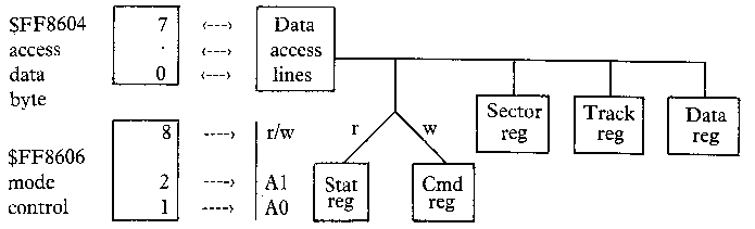
The WD1772A floppy disk controller supports eleven instructions, these should only be loaded into the data byte register when the status bit (bit 5, $FFFA01) is off. The instructions enable head location, reading and writing sectors, tracks and the forced interrupt of a disk operation:
Instruction byte ($FF8604)
Restore
Seek#$00
#$10Seek rate (ms)
+#$00 (2)
+#$01 (3)
+#$02 (5)
+#$03 (6)Verify
+#$04Spin-up
disable
+ #$08Step
Step in
Step out#$20
#$40
#$60Update track
register
+ #$10Read sector
Write sector *#$80
#$A0Multiple sec
+ #$10Add 30 ms delay
+#$04Read address
Read track
Write track *#$C0
#$E0
#$F0Force interrupt #$D0 + #$00 End with no interrupt
+ #$04 Interrupt on index pulse
+ #$08 Immediate interrupt
* May contain + #$02: Write precompensation disabled.
Write sector may also contain + #$01: Write deleted data mark.
Commands are passed to the FDC (and an external HDC), by selecting the appropriate FDC or HDC function (read status / write command, sector, track or data) through the configuration register ($FF8606) and sending instructions or data via the access byte ($FF8604).
Select FDC / HDC function ($FF8606)
| Write #$100 |
FDC #$80 |
DMA #$10 |
#$0 | Read status | Write command |
| #$1 | Track | ||||
| Read #$000 |
HDC #$00 |
1772 #$00 |
#$2 | Sector | |
| #$3 | |||||
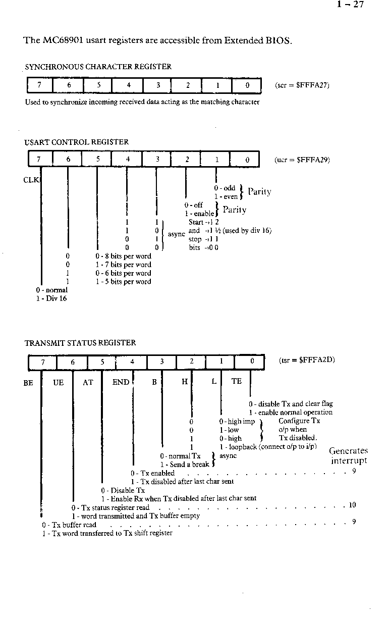
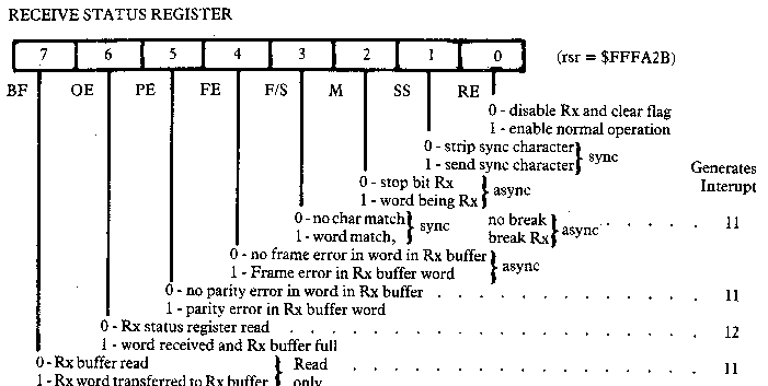
The MC68901 contains a single channel USART capable of operating in full duplex, at a rate of 62.5 Kb/s asynchronous, 1 Mb/s synchronous from an internal or external Baud rate generator. The USART also supports DMA handshake signals and modem control.
There are four timers with independent operation and vectored interrupts, the timers have the following preferred timer uses:
Timer A: Stand alone applications and independent software vendor.
Timer B: Primarily Screen Graphics (hblank, sync etc.)
Timer C: System timing (GSX, GEM, Desktop, etc). Suitable for delays and general timing applications (200Hz).
Timer D: RS232 port baud rate control.
Eight individually programmable I/O pins with interrupt capabilities are also available.
MFP hardware bound interrupts
Priority Function 0 low Parallel port busy GPI (0) 1 RS232 data carrier detect GPI (1) 2 RS232 clear to send GPI (2) 3 GPU operation done GPI (3) 4 RS232 baud rata generator Timer D 5 Timer C (system clock) Timer C 6 Keyboard and MIDI * GPI (4) 7 Disk drive controller GPI (5) 8 Horizontal blanking counter Timer B 9 RS232 transmit error 10 RS232 transmit buffer empty 11 RS232 receive error 12 RS232 receive buffer full 13 Timer A Timer A 14 RS232 ring indicator GPI (6) 15 high Monochrome monitor detect GPI (7)
* Test MC6850 status bit to differentiate between keyboard and MIDI interrupts.
MFP configuration registers
located at address $FFFA01 (16775681)
Offset Function Dec Hex 1 01 General purpose I/O 3 03 Active edge 5 05 Data direction 7 07 Interrupt enable A 9 09 Interrupt enable B 11 0B Interrupt pending A 13 0D Interrupt pending B 15 0F Interrupt in-service A 17 11 Interrupt in-service B 19 13 Interrupt mask A 21 15 Interrupt mask B 23 17 Vector base address 25 19 Timer A control 27 1B Timer B control 29 1D Timers C & D control 31 1F Timer A data 33 21 Timer B data 35 23 Timer C data 37 25 Timer D data 39 27 Sync character 41 29 USART control 43 2B Receiver status 45 2D Transmitter status 47 2F USART data
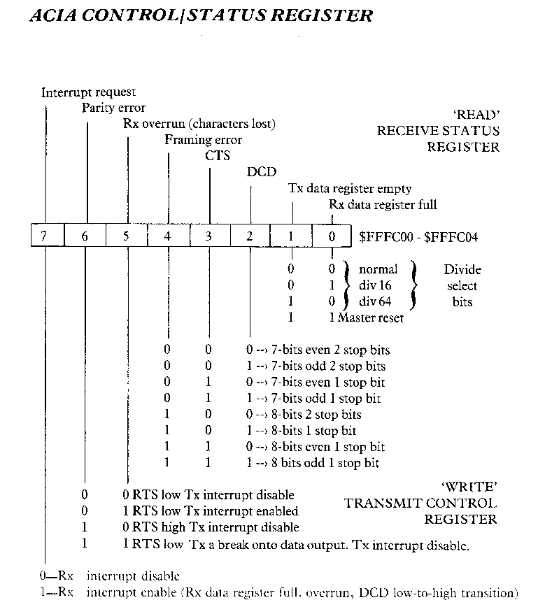
The MC6850 ACIA provides data formatting and control of a serial interface to an 8-bit bidirectional data bus. At the bus interface, the four ACIA registers, the status and receive data (read only) and the control and transmit data (write only) registers, appear as two addressable memory locations.
The programmable ACIA control register, which sets the format of the serial link, is located at $FFFCOO (16776192) for the intelligent keyboard serial communications link, and at $FFFC04 (16776196) for the MIDI interface.
The ACIA supports peripheral/modem control through:
RTS request to send,
CTS clear to send, and
DCD data carrier detect.
Protocols for 8 and 9 bit transmission using an optional odd or even parity, and one or two stop bits, are available through the programmable control register.
The MIDI port may be configured for a second serial port, but the intelligent keyboard interface is not accessible.
The programmable sound generator registers are located as follows:
RAM offset Function bits used reg address base address $FF8800 (16746596) 7 6 5 4 3 2 1 0 0 0 Channel A x x x x x x x x 1 1 Channel A x x x x 2 2 Channel B x x x x x x x x 3 3 Channel B x x x x 4 4 Channel C x x x x x x x x 5 5 Channel C x x x x 6 6 Noise period x x x x x 7 7 Mixer control - I/O enable x x x x x x x x fixed amplitude 8 8 Channel A amplitude M x x x x 9 9 Channel B amplitude M x x x x 10 A Channel C amplitude M x x x x variable amplitude 11 B Envelope period fine x x x x x x x x 12 C Envelope period coarse x x x x x x x x 13 D Envelope shape C R A H 14 E I/O port A (output only) x x x x x x x x 15 F I/O port B (Centronics) x x x x x x x x x = bits used M = mode fixed / variable. C = cycle R = Ramp A = Alternate H = Hold
| R/!W | 1 | ---ST--- DMA |
40 | VCC |
| A1 | 2 | 39 | CLK_8MHZ | |
| !FCS | 3 | 38 | RDY | |
| D0 | 4 | 37 | !ACK | |
| D1 | 5 | 36 | CD0 | |
| D2 | 6 | 35 | CD1 | |
| D3 | 7 | 34 | CD2 | |
| D4 | 8 | 33 | CD3 | |
| D5 | 9 | 32 | CD4 | |
| D6 | 10 | 31 | CD5 | |
| D7 | 11 | 30 | CD6 | |
| D8 | 12 | 29 | CD7 | |
| D9 | 13 | 28 | GND | |
| D10 | 14 | 27 | CA2 | |
| D11 | 15 | 26 | CA1 | |
| D12 | 16 | 25 | CR/!W | |
| D13 | 17 | 24 | !HDCS | |
| D14 | 18 | 23 | HDRQ | |
| D15 | 19 | 22 | !FDCS | |
| GND | 20 | 21 | FDRQ |
| D4 | 1 | ---ST--- MMU |
68 | D3 |
| D5 | 2 | 67 | D2 | |
| D6 | 3 | 66 | D1 | |
| D7 | 4 | 65 | D0 | |
| CLK_16MHZ | 5 | 64 | MAD | |
| CAS_0M | 6 | 63 | MAD | |
| CAS_0L | 7 | 62 | MAD | |
| RAS_0 | 8 | 61 | GND_B | |
| LATCH | 9 | 60 | MAD | |
| VCC | 10 | 59 | MAD | |
| A16 | 11 | 58 | MAD | |
| A17 | 12 | 57 | MAD | |
| A18 | 13 | 56 | MAD | |
| A19 | 14 | 55 | MAD | |
| A20 | 15 | 54 | MAD | |
| A21 | 16 | 53 | DTACK | |
| LDS | 17 | 52 | DE | |
| RAS1 | 18 | 51 | VSYNC | |
| CLK_4MHZ | 19 | 50 | A1 | |
| CLK_8MHZ | 20 | 49 | A2 | |
| CAS_1L | 21 | 48 | A3 | |
| CAS_1M | 22 | 47 | A4 | |
| W/E | 23 | 46 | A5 | |
| DMA | 24 | 45 | A6 | |
| WDAT | 25 | 44 | VCC | |
| UDS | 26 | 43 | A7 | |
| GND_A | 27 | 42 | A8 | |
| CPMCS | 28 | 41 | A9 | |
| DCYC | 29 | 40 | A10 | |
| RDAT | 30 | 39 | A11 | |
| DEV | 31 | 38 | A12 | |
| AS | 32 | 37 | A13 | |
| RAM | 33 | 36 | A14 | |
| R/!W | 34 | 35 | A15 |
| XTL0 | 1 | --ST-- VDC |
40 | VCC |
| 32MHz_XTL1 | 2 | 39 | CLK_16MHZ | |
| D0 | 3 | 38 | !CS | |
| D1 | 4 | 37 | DE | |
| D2 | 5 | 36 | A1 | |
| D3 | 6 | 35 | A2 | |
| D4 | 7 | 34 | A3 | |
| D5 | 8 | 33 | A4 | |
| D6 | 9 | 32 | A5 | |
| D7 | 10 | 31 | R/!W | |
| !LOAD | 11 | 30 | MONO | |
| D8 | 12 | 29 | R0 | |
| D9 | 13 | 28 | R1 | |
| D10 | 14 | 27 | R2 | |
| D11 | 15 | 26 | G0 | |
| D12 | 16 | 25 | G1 | |
| D13 | 17 | 24 | G2 | |
| D14 | 18 | 23 | B0 | |
| D15 | 19 | 22 | B1 | |
| GND | 20 | 21 | B2 |
| VCC | 1 | ---ST--- GLUE |
68 | A13 |
| A14 | 2 | 67 | A12 | |
| A15 | 3 | 66 | A11 | |
| A16 | 4 | 65 | A10 | |
| A17 | 5 | 64 | A9 | |
| A18 | 6 | 63 | A8 | |
| A19 | 7 | 62 | A7 | |
| A20 | 8 | 61 | A6 | |
| A21 | 9 | 60 | A5 | |
| A22 | 10 | 59 | A4 | |
| A23 | 11 | 58 | A3 | |
| AS | 12 | 57 | A2 | |
| FC2 | 13 | 56 | A1 | |
| FC1 | 14 | 55 | R/!W | |
| FC0 | 15 | 54 | CLK_2MHZ | |
| VMA | 16 | 53 | SND_CS | |
| ROM4 | 17 | 52 | GND | |
| ROM3 | 18 | 51 | MFPCS | |
| ROM2 | 19 | 50 | IACK | |
| ROM1 | 20 | 49 | D1 | |
| ROM1 | 21 | 48 | D0 | |
| RESET | 22 | 47 | UDS | |
| RAM | 23 | 46 | LDS | |
| DMA | 24 | 45 | BG0 | |
| DEV | 25 | 44 | MFPINT | |
| FCS | 26 | 43 | CLK500KHZ | |
| BGI | 27 | 42 | 6850CS | |
| RDY | 28 | 41 | BGACK | |
| VPA | 29 | 40 | BR | |
| BERR | 30 | 39 | DE | |
| DTACK | 31 | 38 | VSYNC | |
| IPL1 | 32 | 37 | HSYNC | |
| IPL2 | 33 | 36 | BLANK | |
| CLK_8MHZ | 34 | 35 | GND |