The ANTIC and CTIA chips generate the television display at the rate of 60 frames per second on the NTSC (US) system. The PAL (European) system is different and is described in the section on NTSC vs PAL. Each frame consists of 262 horizontal TV lines and each line is made up of 228 color clocks, as shown in figure VI-3. The 6502 microprocessor runs at 1.79 MHz. This rate was chosen so that one machine cycle is equivalent in length to two color clocks. One clock is approximately equal in width to two TV lines.
In any graphics mode, the display is divided up into small squares or rectangles called pixels (picture elements). The highest resolution graphics mode has a pixel size of 1/2 color clock by 1 TV line. A sample display list is given in section IV.
The current TV line may be determined by reading the vertical counter (VCOUNT). This register gives the line count divided by 2. There are 262 lines per frame so VCOUNT runs from 0 to 130 (0 to 155 on the PAL system). The 0 point occurs near the end of vertical blank (see figure VI.5). Vertical blank (VBLANK) is the time during which the electron beam returns back to the top of the screen in preparation for the next frame. The Atari 800 does not do interlacing, so each frame is identical unless the program which is being executed changes the display. Vertical sync (VSYNC) occurs during the fourth through sixth lines of vertical blank (VCOUNT hex 7D through 7F). This tells the TV set where each frame starts. After VSYNC, there are 16 more lines of VBLANK for a total of 22 lines of VBLANK. The display list jump and wait instruction (to be described later) causes the display list graphics to start at the end of VBLANK.
The ATARI 400/800 comes with a 10K Operating System (OS) in ROM. The OS affects some of the hardware registers, so it will be mentioned from time to time in this manual. Refer to the OS manual for more details. The OS descriptions in this manual apply to the version that was being distributed when this manual was written.
The OS supports most of the hardware graphics modes (BASICS, GRAPHICS, PLOT, and DRAWTO commands). The OS always displays 24 background lines after the end of vertical blank. This convention is used at Atari to compensate for television sets which overscan. Most TV’s are designed so that the edges of the picture are cut off. This is fine for ordinary broadcasts, but with a computer it is essential for all important information to be displayed on the screen. It is fairly common for four to eight color clocks at the right or left edge of the picture to overscan. A TV set that has excessive overscan may have to readjusted to obtain a satisfactory display.
The OS uses 192 TV lines for its display and devotes the remaining 24 lines to overscan. It uses the standard display width of 160 color clocks. The hardware will allow displays of any length, but it is recommended that the standards be followed. The exception might be a border or other information which is merely decorative and not essential to use of the program.
Since many of the hardware registers are write-only and cannot be read the OS has a number of "shadow registers" in RAM.
Every TV frame during vertical blank the OS takes the values in some of its shadow registers, and writes them out to the corresponding hardware register. The OS does attract color shifting on all of the color registers if ATRACT (on OS register) is negative. This is to prevent damage to the TV screen phosphors which can occur if the brightness is turned up too high and the same high-luminance display is left on for a long time. The OS also reads the joysticks and other controllers during vertical blank and stores the results in shadow registers, so that user programs do not have to include code to unpack the data. There are a few interrupt-related registers which the OS changes or reads during interrupt processing. Programs usually access the OS shadow registers instead of accessing the hardware directly. However, the OS shadowing can be disabled by changing the vertical blank and interrupt vectors (see OS manual).
In addition to a Vertical Blank Interrupt, which allows the Microprocessor to synchronize to the vertical TV display, this system also provides a Wait for Horizontal Sync (WSYNC) command that allows the microprocessor to synchronize itself to the TV horizontal line rate. This sync takes effect when the processor writes to an I/0 location called WSYNC, whenever it desires horizontal synchronization. Writing to this address sets a latch which pulls to zero a pin on the microprocessor called READY. When READY goes to zero the microprocessor stops and waits. The latch is automatically reset (returning READY true) at the beginning of the next horizontal blank interval, releasing the microprocessor to resume program execution.
The primary function of the ANTIC chip is to fetch data from memory (independent of the microprocessor) for display on the TV screen. It does this with a technique called "Direct Memory Access" or DMA. It requests the use of the memory address and data bus by sending a signal called HALT to the microprocessor, causing the processor to become "TRI-STATE" (open circuit) all during the next computer cycle. The ANTIC chip then takes over the address bus and reads any data it wishes from memory. Another name for this type of DMA is "cycle stealing". Once initiated, this DMA is completely and automatically controlled by the ANTIC chip without need for further microprocessor intervention.
There are two types of DMA: Playfield and Player-Missile (see Figure II.2). The playfield DMA control circuit on the ANTIC chip resembles a small dumb microprocessor. By halting the main microprocessor it can fetch its own instructions from memory (the display list) addressed by its program counter(display list pointer). Each instruction defines the type (alpha character or memory map), and the resolution (size of bits on the screen), and the location of the data in memory which is to be displayed on the next group of lines.
In order to begin this DMA the main microprocessor must store a display list of instructions in memory, store data to be displayed in memory, tell the ANTIC where the display list is (initialize the display list pointer) and enable the DMA control flags on the ANTIC (DMACTL register).
In addition to the playfield DMA described above, the ANTIC chip simultaneously controls another DMA channel. This type of DMA addresses PLAYER-MISSILE graphics data stored in memory and passes the graphics data on to the CTIA chip graphics registers. This type of DMA (if enabled) occurs automatically, interspersed with the playfield DMA described previously. This PLAYER-MISSILE DMA has no display list or instructions, and is therefore much simpler than the PLAYFIELD DMA.
In addition to the two types of display DMA, the ANTIC chip also generates DMA addresses for the refresh of the dynamic memory RAM used in this system. This is also completely automatic and need be considered by the programmer only if he is concerned with real-time programming where an exact count of the computer cycles is important.
A color-luminance register is used on the CTIA chip for each Player-Missile and Playfield type. Each color-lum register is loaded by the microprocessor with a code representing the desired color and luminance of its corresponding Player-Missile or Playfield type. As the serial data passes through the CTIA chip it is "impressed" with the color and luminance values contained in these registers, before being sent to the TV display. In areas of the screen where there are no objects the background color (COLBK) is displayed. The CTIA also does collision detection (to be described later).
When moving objects, such as players and missiles, overlap on the TV screen (with each other or with Playfield) a decision must be made as to which object shows in front of the other. Objects which appear to pass in front of others are said to have Priority over them. Priority is assigned to all objects by the CTIA chip before the serial data from each object is combined with the other objects and sent to the TV screen.
The priority of objects can be controlled by the microprocessor by writing into the control register PRIOR. The functions of the bits in this register are given in the table in the PRIOR register description in section III.
The players and missiles are small objects which can be moved quickly in the horizontal direction by changing their position registers. They are called players and missiles because they were originally designed to be used in games for objects such as aeroplanes and bullets. However, there are many other possible applications for them. The four player-missile color registers, in con]unction with the four playfield color registers and the background color register, make it possible to display 9 different colors at the same time.
Figure II.2 OBJECT DISPLAY SOURCES
There are a total of four players and four missiles. The four missiles may be grouped together and used as a 5th player. These objects are positioned horizontally by 8 horizontal position registers (HPOS (X)). These registers may be reloaded at any time by the processor, allowing an object to be replicated many times across a horizontal TV line.
The shape of a player-missile is determined by the data in its graphics register (GRAF (X)). Players have independent 8 bit graphics registers. The four missiles have 2 bit registers (located within one address). These registers may also be reloaded at any time by the processor, although they are usually changed during horizontal blank time. The data in each graphics register is placed on the display whenever the horizontal sync counter equals the corresponding horizontal position register. The same data will be displayed every line unless the graphic registers are reloaded with new data.
The player-missile graphic registers may be reloaded by the micro-processor (GRAF (X)), or automatically from memory with direct memory access (DMA) (see figure II.3). The programmer must place the object graphics in memory, write the player-missile base address (PMBASE), and enable player-missile DMA (DMACTL, GRACTL). The transfer of object graphics from memory to display is then fully automatic.
PMBASE specifies the most significant byte (MSB) of the address of the player-missile graphics. The location of the graphics for each object is determined by adding an offset to PMBASE *256 (decimal). The bytes between the base address and the missile data are not used by ANTIC, so they are available to the programmer.
Only the five most significant bits of PMBASE are used with single-line resolution and the six most significant bits are used with two-line resolution. This means that the location of the graphics in memory is restricted to certain page boundaries. Two-line resolution means that each byte of data is repeated for two lines. (see DMACTL, bit 4). 640 (decimal) bytes (5x128) are required for two-line resolution and 1280 bytes (5x256) for one-line resolution.
Each byte in the player graphics area represents eight pixels which are to be displayed on the corresponding line(s) of the TV screen. A 1 indicates that the player s color-lum is to be displayed in that pixel. The graphics may be anything, not just rectangles like the ones in figure II.3. The player graphics may fill the entire height of the screen or they may be only a couple of lines high if the rest of the display data is all 0's. Each byte in the missile display also represents eight pixels, two pixels for each missile. Each pixel may be 1, 2, or 4 color clocks, and is determined by the SIZE registers.
Playfield is always generated by DMA. There are four playfields, each identified by its own color-lum register and collision detection. Playfield is generated by two different DMA techniques: memory map and character. Both methods provide lists of instructions in memory, independent of the player-missile generation.
Figure II.2: PLAYER – MISSILE DMA
Unlike players and missiles, there are no horizontal position registers for playfield. Each player can only have one byte of display per line. Playfield, on the other hand, may require up to 48 bytes per line because it can fill the entire width of the screen.
There are three different playfield widths: narrow (128 color clocks), standard (160 color clocks), and wide (192 color clocks).
The width is selected by storing into DMACTL. The advantage of a narrower width is that less RAM is required and fewer machine cycles are stolen for DMA. The OS graphics modes use the standard screen width.
The display list is a sequence of display instructions stored in memory. These instructions are either one (1) byte or three (3) bytes long. The display list can be considered a display program, and the Display List Counter that fetches these instructions can be thought of as a display program counter. (10 bit counter plus 6 bit base register.)
The display list counter can be initialized by writing to DLISTH and DLISTL. (or OS shadow registers SDLSTH and SDLSTL). Once initialized this counter value is used to address the display list, fetch the instruction, display one (1) to sixteen (16) lines of data on the TV screen, increment the Display List Counter, fetch the next display instruction, and so on automatically without microprocessor control (see DLISTL and DLISTH). DLISTL and DLISTH should be altered only during vertical blank or when DMA is disabled (see DMACTL).
Each instruction defines the type (alpha character or memory map) and the resolution (size of bits on screen) and the location of data in memory to be displayed for a group (1 to 16) of lines. Each group of lines is called a display block.
THE DISPLAY LIST CANNOT CROSS A 1K BYTE MEMORY BOUNDARY UNLESS A JUMP INSTRUCTION IS USED.
DLISTH MSB DLISTL LSB D7 D6 D5 D4 D3 D2 D1 D0 D7 D6 D5 D4 D3 D2 D1 D0 15 14 13 12 11 10 9 8 7 6 5 4 3 2 1 0 Fixed (6 bits) Counter (10 bits)
DISPLAY LIST COUNTER
Each instruction consists of either an opcode only, or of an opcode followed by two (2) bytes of operand.
Opcode Single Byte Display Instruction Opcode Triple Byte Display Instruction Operand Operand
The opcode is always fetched first and placed in the Instruction Register. This opcode defines the type of instruction (1 or 3 bytes) and will cause two more bytes to be fetched if needed. If fetched, these next two (2) bytes will be placed in the Memory Scan Counter, or in the Display List Counter (if the instruction is a Jump).
This register is loaded with the opcode of the current display list instruction. It cannot be accessed directly by the programmer. There are three basic types of display list instructions: blank, jump, and display.
| Blank | D7 | D6 | D5 | D4 | 0 | 0 | 0 | 0 | |
| (1-byte) | This instruction is used to create 1 to 8 blank lines on the display (background color). | ||||||||
| 0 | 0 | 0 | 0 | Blank | |||||
| 0-7 = 1-8 blank lines | |||||||||
| 1 = display list instruction interrupt | |||||||||
| Jump | D7 | D6 | X | X | 0 | 0 | 0 | 1 | |
| (3-bytes) | This instruction is used to reload the
Display List Counter. The next two bytes specify the address to be loaded (LSB first). |
||||||||
| 0 | 0 | 0 | 1 | Jump | |||||
| X | X | Don't care | |||||||
| 0 | Jump (creates one blank line on display) | ||||||||
| 1 | As above then wait until end of next vertical blank | ||||||||
| 1 = display list instruction interrupt | |||||||||
| Display | D7 | D6 | D5 | D4 | D3 | D2 | D1 | D0 | |
| (1 or 3 bytes) | Display mode 2 to F (character or graphics, see later) | ||||||||
| 1 = Horizontal Scroll Enable | |||||||||
| 1 = Vertical Scroll Enable | |||||||||
| 0 = 1-byte instruction, 1 = 3-byte instruction. | |||||||||
| 1 = display list instruction interrupt | |||||||||
Figure II.3: DISPLAY INSTRUCTION OPCODES
Bit 7 of a display list instruction can be set to create a display list interrupt if bit 7 of NMIEN is set. The display list interrupt code can change the colors or graphics during the middle of the TV display. The type of interrupt is determined by checking NMIST. NMIRES clears NMIST. The current OS will vector through VDSLST (Hex 200 and 201) to the user's display list interrupt routine. See the OS manual for programming details.
Bits 5 and 4 of a display type of display list instructions are used to enable vertical and horizontal scrolling. The amount of scrolling depends on the values in the VSCROL and HSCROL registers (to be described later).
This counter is not directly accessible by the programmer. It is loaded with the value in the last 2 bytes of a 3 byte (non-Jump) instruction.
This counter points to the location (address) in memory of data to be directly displayed (memory map display) or to the location of character name strings to be indirectly displayed (character display).
A single byte instruction does not reload this counter. This implies a continuation in memory of data to be displayed from that displayed by the previous instruction. Since this counter really consists of 4 bits of register and 12 of actual counter, a continuous memory block cannot cross 4K byte memory boundaries, unless the counter is repositioned with a 3-byte Load Memory Scan Counter instruction.
MSB third byte of 3 byte instruction LSB Second byte of 3 byte instruction D7 D6 D5 D4 D3 D2 D1 D0 D7 D6 D5 D4 D3 D2 D1 D0 15 14 13 12 11 10 9 8 7 6 5 4 3 2 1 0 Fixed (4 bits) Counter (12 bits)
60 bits of collision register are provided to detect and store overlap (hits) between players, missiles and playfield. These collisions can be read by the microprocessor from addresses D000 through D00F. There are no bits for missile to missile collisions.
- 16 bits for Missile to Playfield
- 16 bits for Player to Playfield
- 16 bits for Missile to Player
- 12 bits for Player to Player (P0 to P0 always reads as zero, etc.)
The 1/2 clock memory map mode (IR code 1111) and the 1/2 clock Character mode (IR codes 0011 and 0010) are both playfield type 2 collisions and will be stored in bit 2 of the playfield collision registers.
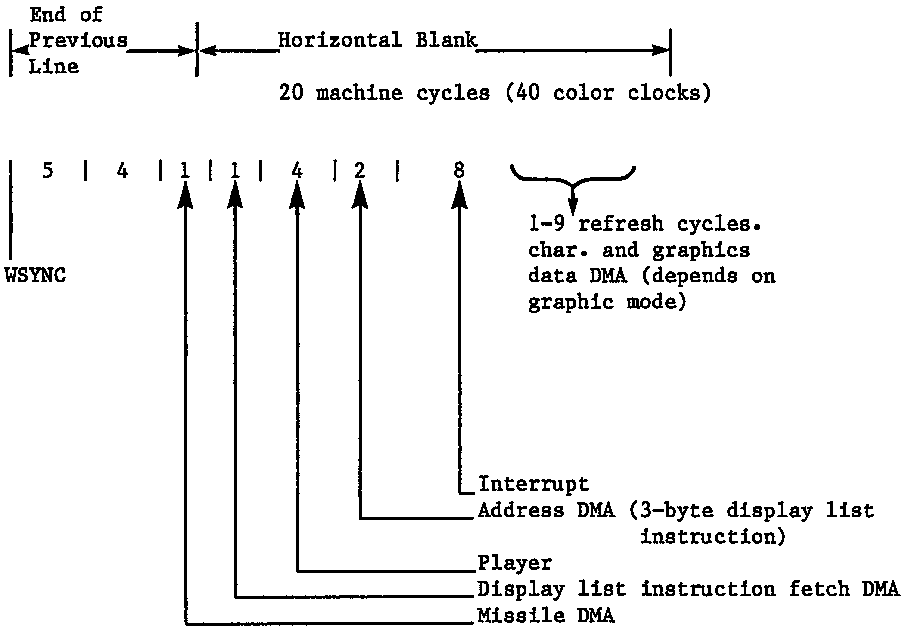
When DMA is enabled, cycles are stolen at the times shown below.
[The diagram above is not very clear. According to an Atari diagram of the ANTIC cycles:]
| <--End of previous line--> | <-- this line--> | ||||||
| <--WSYNC | <--Horizontal Blank--> 20 machine cycles (40 color clocks) |
<---------Display ---------> | |||||
| 5 | 4 | 1 | 1 | 4 | 2 | 8 | |
| ^ | |
^ | |
^ | |
^ | |
^ | |
1-9
refresh cycles, plus char. and graphics data DMA (depends on graphic mode) |
||
| | | | | | | | | Interrupt | |||
| | | | | | | Address DMA (on 3-byte display list instructions only) |
||||
| | | | | Player | |||||
| | | Display list instruction fetch DMA | ||||||
| Missile DMA | |||||||
There are two versions of the ATARI 800: the NTSC (United States TV standard) and PAL (one of the European TV standards). The PAL system has been designed so that most programs will run without being modified. However, some differences may be noticeable. There is a hardware register (PAL) which a program can read to determine which type of system it is running on and adjust accordingly.
The PAL TV has a slower frame rate (50 Hz. instead of 60 Hz.) so games will be slower unless an adjustment is made. PAL has more TV lines per frame (312 instead of 262). The Atari 800 hardware compensates for this by adding extra lines at the beginning of vertical blank. Display lists do not have to be altered. However, their actual vertical height will be shorter. PAL ATARI 800 colors are similar to NTSC because of a hardware modification.