Preliminary Data
32 bit architecture with 10 MIPS performance
2 Kbytes 50 ns RAM on chip
Four 5/10/20 Mbits/sec INMOS serial links
32 bit configurable memory interface
Directly addresses 4 Gbytes at 26.6 Mbytes/sec
Hardware scheduler for concurrent programs
Sub-microsecond context switch
Internal timers for real time processing
External event interrupt
Sub-microsecond typical interrupt latency
Support for run-time error diagnostics
Boots from communication link or ROM
On-chip DRAM controller
Optional external memory wait states
Internal program continues during DMA
6.4 Mbytes/sec total link data rate
Single 5 MHz clock input
Single +5V ±10% power supply, less than 1 Watt
High speed multi processor systems
Real time processing
Microprocessor applications
Workstations and workstation clusters
Image processing
Graphics processing
Accelerator processors
Distributed databases
Supercomputers
System simulation
Digital signal processing
Telecommunications
Robotics
Fault tolerant systems
Medical instrumentation
Pattern recognition
Artificial intelligence
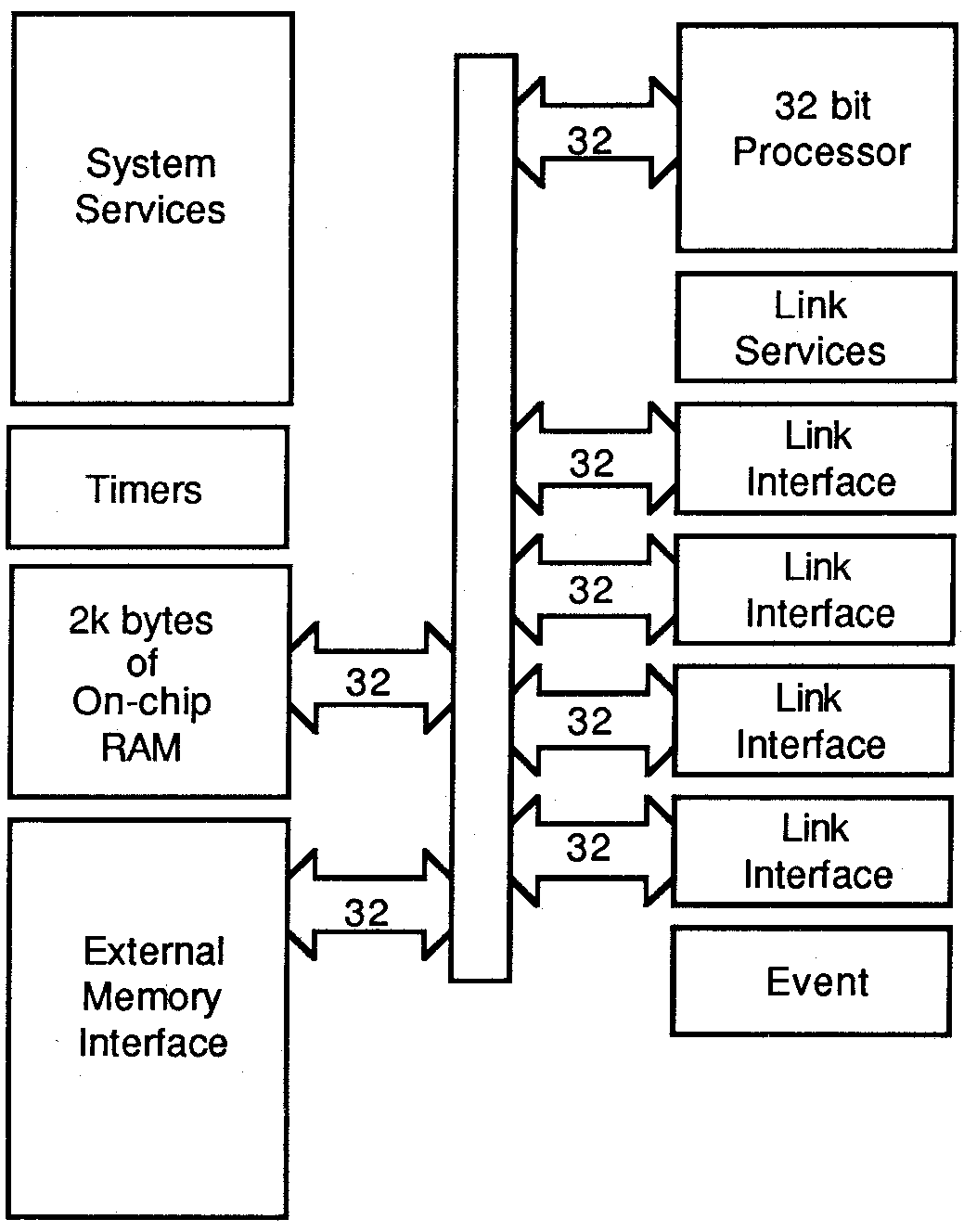
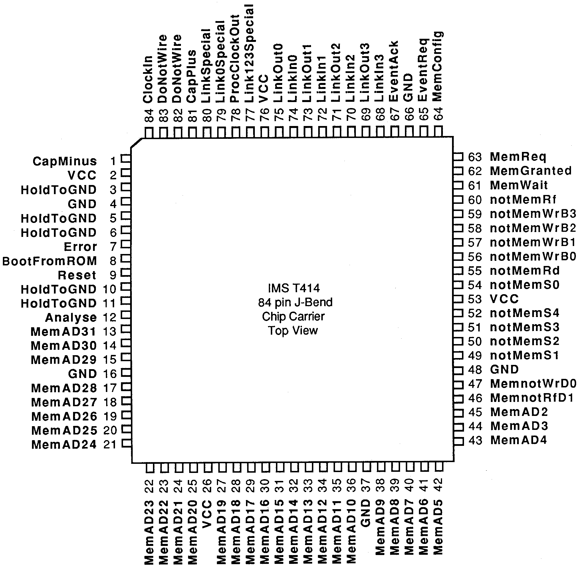
The IMS T414 transputer is a 32 bit microcomputer with 2 Kbytes on-chip RAM for high speed processing, a configurable memory interface and four standard INMOS communication links. The instruction set achieves efficient implementation of high level languages and provides direct support for the occam model of concurrency when using either a single transputer or a network. Procedure calls, process switching and typical interrupt latency are sub-microsecond. The IMS T414 provides high performance arithmetic and microcode support for floating point operations. A device running at 20 MHz achieves an instruction throughput of 10 MIPS.
The IMS 7414 can directly access a linear address space of 4 Gbytes. The 32 bit wide memory interface uses multiplexed data and address lines and provides a data rate of up to 4 bytes every 150 nanoseconds (26.6 Mbytes/sec) for a 20 MHz device. A configurable memory controller provides all timing, control and DRAM refresh signals for a wide variety of mixed memory systems.
The INMOS communication links allow networks of transputers to be constructed by direct point to point connections with no external logic. The links support the standard operating speed of 10 Mbits per second, but also operate at 5 and 20 Mbits per second.
The IMS T414 is designed to implement the occam language, detailed in the occam Reference Manual, but also efficiently supports other languages such as C, Pascal and Fortran. Access to the transputer at machine level is seldom required, but if necessary refer to the Transputer Instruction Set Manual and Compiler Writers Guide.
This data sheet supplies hardware implementation and characterisation details for the IMS T414. It is intended to be read in conjunction with the Transputer Reference Manual, which details the architecture of the transputer and gives an overview of occam.
For convenience of description, the IMS T414 operation is split into the basic blocks shown in the Block Diagram.
IMS T414 Block Diagram
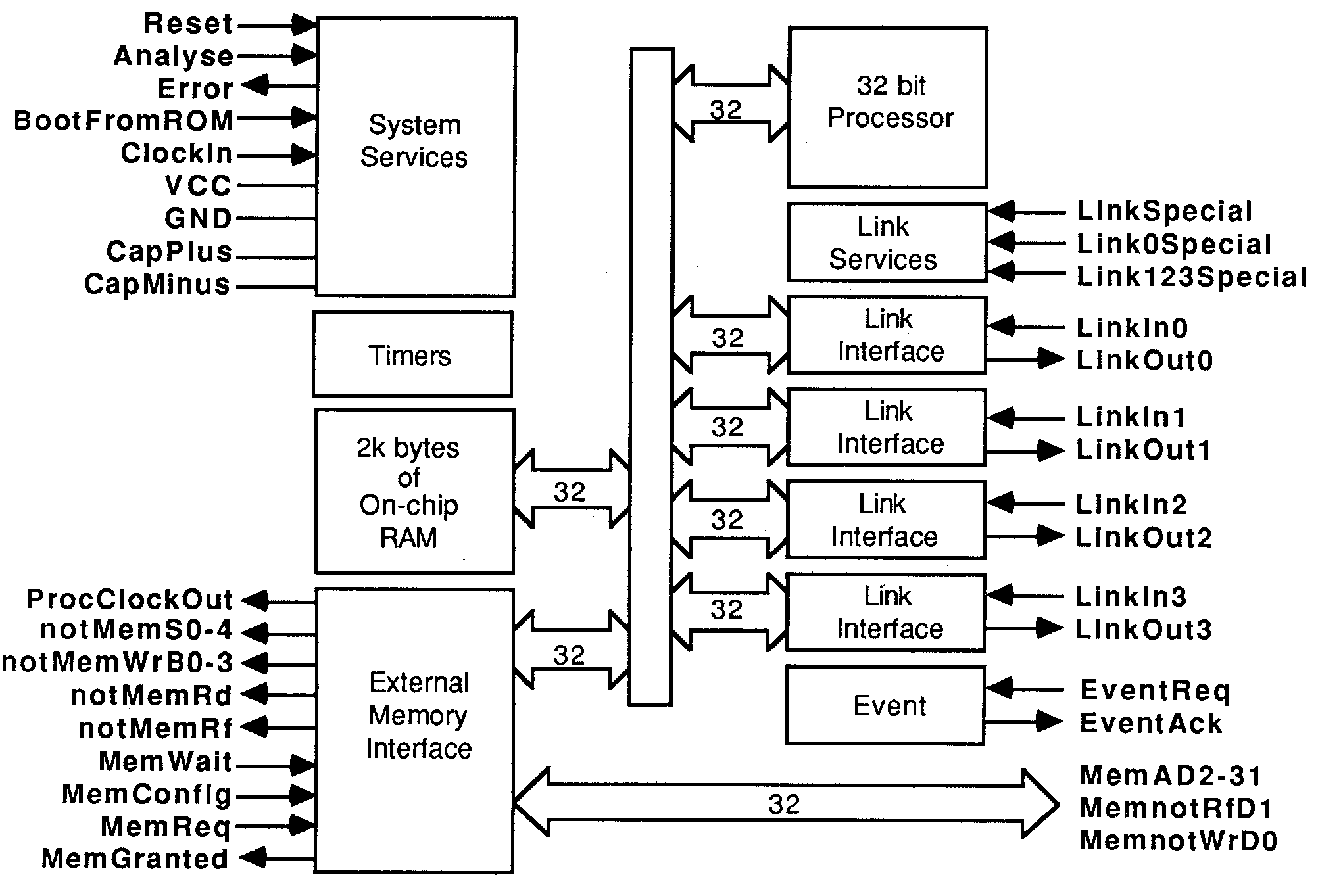
The Error pin is connected directly to the internal Error flag and follows the state of that flag. If Error is high it indicates an error in one of the processes caused, for example, by arithmetic overflow, divide by zero, array bounds violation or software setting the flag directly (section 3.7.2).
A process can be programmed to stop if Error is set; it cannot then transmit erroneous data to other processes, but processes which do not require that data can still be scheduled. Eventually all processes which rely, directly or indirectly, on data from the process in error will stop through lack of data.
By setting the HaltOnError flag the transputer itself can be programmed to halt if Error becomes set. If Error becomes set after HaltOnError has been set, all processes on that transputer will cease but will not necessarily cause other transputers in a network to halt. Setting HaltOnError after Error will not cause the transputer to halt; this allows.Reset and Analyse to function with the flags in indeterminate states.
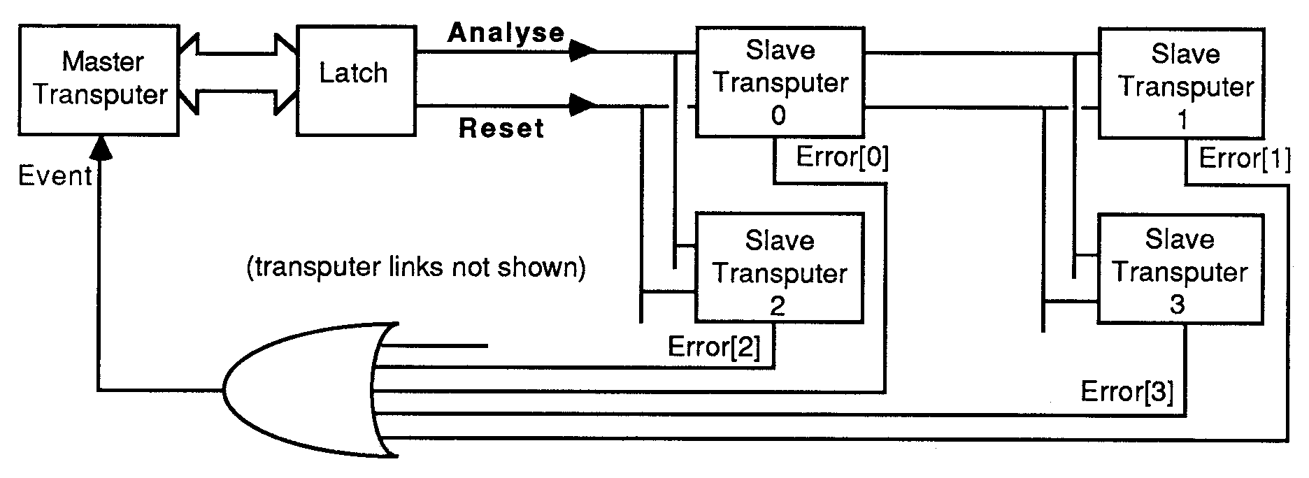
An alternative method of error handling is to have the errant process or transputer cause all transputers to halt. This can be dcne by applying the Error output signal of the errant transputer to the EventReq pin of a suitably programmed master transputer. Since the process state is preserved when stopped by an error, the master transputer can then use the Analyse function to debug the fault.
Error checks can be removed completely to optimise the performance of a proven program; any unexpected error then occurring will have an undefined effect.
If a high priority process pre-empts a low priority one, status of the Error and HaltOnError flags is saved for the duration of the high priority process and restored at the conclusion of it. Status of the Error flag is transmitted to the high priority process but the HaltOnError flag is cleared before the process starts. Either flag can be altered in the process without upsetting the error status of any complex operation being carried out by the pre-empted low priority process.
In the event of a transputer halting because of HaltOnError, the links will finish outstanding transfers before shutting down. If Analyse is asserted then all inputs continue, but outputs will not make another access to memory for data. Memory refresh will continue to take place.
After halting due to Error changing from 0 to 1 whilst HaltOnError is set, register I points one or two bytes past the instruction which set Error. After halting due to Analyse being taken high, register I points one byte past the instruction being executed. In both cases I will be copied to register A.
Error Handling in a Multi-Transputer System
The IMS 7414 has 2 Kbytes of fast internal memory for high rates of data throughput. Each internal memory access takes one processor cycle ProcClockOut (section 6.1). The transputer can also access 4 Gbytes of external memory space. Internal and external memory are part of the same linear address space.
Transputer memory is byte addressed, with words aligned on four-byte boundaries. The least significant byte of a word is the lowest addressed byte.
The bits in a byte are numbered 0 to 7, with bit 0 the least significant. The bytes are numbered from 0, with byte 0 the least significant. In general, wherever a value is treated as a number of component values, the components are numbered in order of increasing numerical significance, with the least significant component numbered 0. Where values are stored in memory, the least significant component value is stored at the lowest (most negative) address.
Internal memory starts at the most negative address 080000000 and extends to #800007FF. User memory begins at #80000048; this location is given the name MemStart.
A reserved area at the bottom of internal memory is used to implement link and event channels.
Two words of memory are reserved for timer use, TPtrLoc0 for high priority processes and TPtrLoc1 for low priority processes. They either indicate the relevant priority timer is not in use or point to the first process on the timer queue at that priority level.
Values of certain processor registers for the current low priority process are saved in the reserved IntSaveLoc locations when a high priority process pre-empts a low priority one.
External memory space starts at #80000800 and extends up through #00000000 to #7FFFFFFF. Memory configuration data and ROM bootstrapping code must be in the most positive address space, starting at #7FFFFF6C and #7FFFFFFE respectively. Address space immediately below this is conventionally used for ROM based code.
| Machine Map Byte Address |
Occam Map Word offset |
|||
| #80000000 | Link 0 Output | #00 | (Base of memory) | |
| #80000004 | Link 1 Output | #01 | ||
| #80000008 | Link 2 Output | #02 | ||
| #8000000C | Link 3 Output | #03 | ||
| #80000010 | Link 0 Input | #04 | ||
| #80000014 | Link 1 Input | #05 | ||
| #80000018 | Link 2 Input | #06 | ||
| #8000001C | Link 3 Input | #07 | ||
| #80000020 | Event | #08 | ||
| #80000024 | TPtrLoc0 | #09 | ||
| #80000028 | TPtrLoc1 | #0A | ||
| #8000002C | WdescIntSaveLoc | See Note 1 | ||
| #80000030 | IptrIntSaveLoc | |||
| #80000034 | AregIntSaveLoc | |||
| #80000038 | BregIntSaveLoc | |||
| #8000003C | CregIntSaveLoc | |||
| #80000040 | STATUSIntSaveLoc | |||
| #80000044 | EregIntSaveLoc | |||
| #80000048 | MemStart | #12 | ||
| #80000800 | Start of external memory | #0200 | ||
| #00000000 | ||||
| #7FFFFF6C to #7FFFFFF8 |
Memory configuration |
|||
| #7FFFFFFE | Reset Inst | (ResetCodePtr) | ||
| High Byte | Low Byte | |||
Memory Map
Notes
1 These locations are used as auxiliary processor registers and should not be manipulated by the user. Like processor registers, their contents may be useful for implementing debugging tools (see Analyse section 4.7). For details see Compiler Writers Guide.

| Symbol | Parameter | Min. | Nom. | Max. | Units | Notes |
| qJA | Junction to ambient thermal resistance | . | . | 35 | °C/W | 1 |
Notes:
1. Measured in still air.
| Symbol | Parameter | Min. | Nom. | Max. | Units | Notes |
| qJA | Junction to ambient thermal resistance | . | . | 35 | °C/W | 1 |
Notes:
1. Measured in still air.